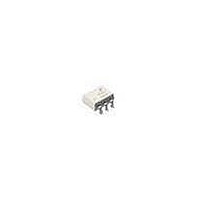
4N35FM Fairchild Semiconductor, 4N35FM Datasheet - Page 5

4N35FM
Manufacturer Part Number
4N35FM
Description
Transistor Output Optocouplers Optocoupler Phototransistor
Manufacturer
Fairchild Semiconductor
Datasheet
1.4N35SR2M.pdf
(9 pages)
Specifications of 4N35FM
Maximum Input Diode Current
60 mA
Maximum Reverse Diode Voltage
6 V
Output Device
Phototransistor
Output Type
DC
Configuration
1 Channel
Input Type
DC
Maximum Collector Emitter Voltage
30 V
Maximum Collector Emitter Saturation Voltage
0.3 V
Isolation Voltage
5300 Vrms
Maximum Forward Diode Voltage
1.5 V
Maximum Power Dissipation
250 mW
Maximum Operating Temperature
+ 100 C
Minimum Operating Temperature
- 55 C
Package / Case
PDIP-6
Lead Free Status / RoHS Status
Lead free / RoHS Compliant
©2005 Fairchild Semiconductor Corporation
4NXXM, H11AXM Rev. 1.0.2
Typical Performance Curves
1000
100
0.1
1.4
1.3
1.2
1.1
1.0
0.9
0.8
0.7
0.6
0.5
0.4
0.3
0.2
0.1
10
1
0.1
10
Fig. 7 Switching Speed vs. Load Resistor
I
V
T
F
A
CC
= 10 mA
= 25 C
Fig. 9 Normalized t
100
INPUT
= 10 V
R
BE
R-LOAD RESISTOR (k
- BASE RESISTANCE (k
1
I
F
T
off
T
T
1000
R
on
r
TEST CIRCUIT
BE
T
f
off
vs. R
Figure 11. Switching Time Test Circuit and Waveforms
10
I
V
C
CC
10000
BE
= 10V
OUTPUT
R
V
I
R
(Continued)
C
CC =
L
L
= 2 mA
Adjust I
= 100
10 V
F
to produce I
100000
100
C
= 2 mA
5
10000
0.001
1000
0.01
100
0.1
5.0
4.5
4.0
3.5
3.0
2.5
2.0
1.5
1.0
0.5
10
1
10%
90%
0
10
V
T
t
on
A
CE
= 25 C
Fig. 10 Dark Current vs. Ambient Temperature
= 10 V
20
t
r
WAVE FORMS
T
Fig. 8 Normalized t
100
A
R
BE
- AMBIENT TEMPERATURE ( C)
- BASE RESISTANCE (k
40
t
t
f
off
INPUT PULSE
OUTPUT PULSE
1000
60
on
vs. R
10000
BE
www.fairchildsemi.com
V
I
R
80
C
CC =
L
= 2 mA
= 100
10 V
100000
100


