MA160014 Microchip Technology, MA160014 Datasheet - Page 106
MA160014
Manufacturer Part Number
MA160014
Description
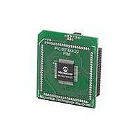
MOD PLUG-IN 44PIN PIC18LF45K22
Manufacturer
Microchip Technology
Series
PIC® XLP™ 18Fr
Datasheet
1.PIC18F26J13-ISS.pdf
(496 pages)
Specifications of MA160014
Accessory Type
Plug-In Module (PIM) - PIC18LF45K10
Product
Microcontroller Modules
Data Bus Width
8 bit
Core Processor
PIC18LF45K22
Interface Type
I2C, SPI
Operating Supply Voltage
1.8 V to 5.5 V
Lead Free Status / RoHS Status
Lead free / RoHS Compliant
For Use With/related Products
PICDEM PIC18 Explorer, DM183032
Lead Free Status / Rohs Status
Lead free / RoHS Compliant
Available stocks
Company
Part Number
Manufacturer
Quantity
Price
Company:

Part Number:
MA160014
Manufacturer:
Microchip Technology
Quantity:
135
Company:
Part Number:
MA160014
Manufacturer:
MICROCHIP
Quantity:
12 000


PIC18(L)F2X/4XK22
REGISTER 7-1:
DS41412D-page 106
bit 7
Legend:
R = Readable bit
S = Bit can be set by software, but not cleared
-n = Value at POR
bit 7
bit 6
bit 5
bit 4
bit 3
bit 2
bit 1
bit 0
Note 1:
EEPGD
R/W-x
When a WRERR occurs, the EEPGD and CFGS bits are not cleared. This allows tracing of the
error condition.
EEPGD: Flash Program or Data EEPROM Memory Select bit
1 = Access Flash program memory
0 = Access data EEPROM memory
CFGS: Flash Program/Data EEPROM or Configuration Select bit
1 = Access Configuration registers
0 = Access Flash program or data EEPROM memory
Unimplemented: Read as ‘0’
FREE: Flash Row (Block) Erase Enable bit
1 = Erase the program memory block addressed by TBLPTR on the next WR command
0 = Perform write-only
WRERR: Flash Program/Data EEPROM Error Flag bit
1 = A write operation is prematurely terminated (any Reset during self-timed programming in normal
0 = The write operation completed
WREN: Flash Program/Data EEPROM Write Enable bit
1 = Allows write cycles to Flash program/data EEPROM
0 = Inhibits write cycles to Flash program/data EEPROM
WR: Write Control bit
1 = Initiates a data EEPROM erase/write cycle or a program memory erase cycle or write cycle.
0 = Write cycle to the EEPROM is complete
RD: Read Control bit
1 = Initiates an EEPROM read (Read takes one cycle. RD is cleared by hardware. The RD bit can only
0 = Does not initiate an EEPROM read
R/W-x
CFGS
(cleared by completion of erase operation)
operation, or an improper write attempt)
(The operation is self-timed and the bit is cleared by hardware once write is complete.
The WR bit can only be set (not cleared) by software.)
be set (not cleared) by software. RD bit cannot be set when EEPGD = 1 or CFGS = 1.)
EECON1: DATA EEPROM CONTROL 1 REGISTER
W = Writable bit
‘1’ = Bit is set
U-0
—
R/W-0
FREE
Preliminary
U = Unimplemented bit, read as ‘0’
‘0’ = Bit is cleared
WRERR
R/W-x
(1)
WREN
R/W-0
2010 Microchip Technology Inc.
x = Bit is unknown
R/S-0
WR
R/S-0
RD
bit 0
Related parts for MA160014
Image
Part Number
Description
Manufacturer
Datasheet
Request
R

Part Number:
Description:
Manufacturer:
Microchip Technology Inc.
Datasheet:
Part Number:
Description:
Manufacturer:
Microchip Technology Inc.
Datasheet:
Part Number:
Description:
Manufacturer:
Microchip Technology Inc.
Datasheet:
Part Number:
Description:
Manufacturer:
Microchip Technology Inc.
Datasheet:
Part Number:
Description:
Manufacturer:
Microchip Technology Inc.
Datasheet:
Part Number:
Description:
Manufacturer:
Microchip Technology Inc.
Datasheet:
Part Number:
Description:
Manufacturer:
Microchip Technology Inc.
Datasheet:
Part Number:
Description:
Manufacturer:
Microchip Technology Inc.
Datasheet: