MA160014 Microchip Technology, MA160014 Datasheet - Page 96
MA160014
Manufacturer Part Number
MA160014
Description
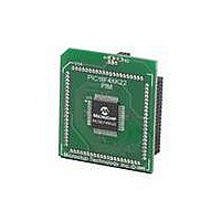
MOD PLUG-IN 44PIN PIC18LF45K22
Manufacturer
Microchip Technology
Series
PIC® XLP™ 18Fr
Datasheet
1.PIC18F26J13-ISS.pdf
(496 pages)
Specifications of MA160014
Accessory Type
Plug-In Module (PIM) - PIC18LF45K10
Product
Microcontroller Modules
Data Bus Width
8 bit
Core Processor
PIC18LF45K22
Interface Type
I2C, SPI
Operating Supply Voltage
1.8 V to 5.5 V
Lead Free Status / RoHS Status
Lead free / RoHS Compliant
For Use With/related Products
PICDEM PIC18 Explorer, DM183032
Lead Free Status / Rohs Status
Lead free / RoHS Compliant
Available stocks
Company
Part Number
Manufacturer
Quantity
Price
Company:

Part Number:
MA160014
Manufacturer:
Microchip Technology
Quantity:
135
Company:
Part Number:
MA160014
Manufacturer:
MICROCHIP
Quantity:
12 000


PIC18(L)F2X/4XK22
FIGURE 6-2:
6.2
Several control registers are used in conjunction with
the TBLRD and TBLWT instructions. These include the:
• EECON1 register
• EECON2 register
• TABLAT register
• TBLPTR registers
6.2.1
The EECON1 register
register for memory accesses. The EECON2 register is
not a physical register; it is used exclusively in the
memory
EECON2 will read all ‘0’s.
The EEPGD control bit determines if the access will be
a program or data EEPROM memory access. When
EEPGD is clear, any subsequent operations will
operate on the data EEPROM memory. When EEPGD
is set, any subsequent operations will operate on the
program memory.
The CFGS control bit determines if the access will be
to the Configuration/Calibration registers or to program
memory/data EEPROM memory. When CFGS is set,
subsequent operations will operate on Configuration
registers regardless of EEPGD (see
“Special Features of the
memory selection access is determined by EEPGD.
DS41412D-page 96
Note 1: During table writes the Table Pointer does not point directly to Program Memory. The LSBs of TBLPRTL
Control Registers
TBLPTRU
write
EECON1 AND EECON2 REGISTERS
(TBLPTR<MSBs>)
Program Memory
actually point to an address within the write block holding registers. The MSBs of the Table Pointer deter-
mine where the write block will eventually be written. The process for writing the holding registers to the
program memory array is discussed in
and
Table Pointer
TBLPTRH
TABLE WRITE OPERATION
erase
(Register
CPU”). When CFGS is clear,
(1)
sequences.
TBLPTRL
6-1) is the control
Section 24.0
Reading
Preliminary
Section 6.5 “Writing to Flash Program
Instruction: TBLWT*
Program Memory
The FREE bit allows the program memory erase
operation. When FREE is set, an erase operation is
initiated on the next WR command. When FREE is
clear, only writes are enabled.
The WREN bit, when set, will allow a write operation.
The WREN bit is clear on power-up.
The WRERR bit is set by hardware when the WR bit is
set and cleared when the internal programming timer
expires and the write operation is complete.
The WR control bit initiates write operations. The WR
bit cannot be cleared, only set, by firmware. Then WR
bit is cleared by hardware at the completion of the write
operation.
Note:
Note:
During normal operation, the WRERR is
read as ‘1’. This can indicate that a write
operation was prematurely terminated by
a Reset, or a write operation was
attempted improperly.
The EEIF interrupt flag bit of the PIR2
register is set when the write is complete.
The EEIF flag stays set until cleared by
firmware.
Holding Registers
2010 Microchip Technology Inc.
Memory”.
Table Latch (8-bit)
TABLAT
Related parts for MA160014
Image
Part Number
Description
Manufacturer
Datasheet
Request
R

Part Number:
Description:
Manufacturer:
Microchip Technology Inc.
Datasheet:
Part Number:
Description:
Manufacturer:
Microchip Technology Inc.
Datasheet:
Part Number:
Description:
Manufacturer:
Microchip Technology Inc.
Datasheet:
Part Number:
Description:
Manufacturer:
Microchip Technology Inc.
Datasheet:
Part Number:
Description:
Manufacturer:
Microchip Technology Inc.
Datasheet:
Part Number:
Description:
Manufacturer:
Microchip Technology Inc.
Datasheet:
Part Number:
Description:
Manufacturer:
Microchip Technology Inc.
Datasheet:
Part Number:
Description:
Manufacturer:
Microchip Technology Inc.
Datasheet: