MA160014 Microchip Technology, MA160014 Datasheet - Page 404
MA160014
Manufacturer Part Number
MA160014
Description
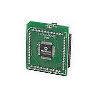
MOD PLUG-IN 44PIN PIC18LF45K22
Manufacturer
Microchip Technology
Series
PIC® XLP™ 18Fr
Datasheet
1.PIC18F26J13-ISS.pdf
(496 pages)
Specifications of MA160014
Accessory Type
Plug-In Module (PIM) - PIC18LF45K10
Product
Microcontroller Modules
Data Bus Width
8 bit
Core Processor
PIC18LF45K22
Interface Type
I2C, SPI
Operating Supply Voltage
1.8 V to 5.5 V
Lead Free Status / RoHS Status
Lead free / RoHS Compliant
For Use With/related Products
PICDEM PIC18 Explorer, DM183032
Lead Free Status / Rohs Status
Lead free / RoHS Compliant
Available stocks
Company
Part Number
Manufacturer
Quantity
Price
Company:

Part Number:
MA160014
Manufacturer:
Microchip Technology
Quantity:
135
Company:
Part Number:
MA160014
Manufacturer:
MICROCHIP
Quantity:
12 000


PIC18(L)F2X/4XK22
SUBWFB
Syntax:
Operands:
Operation:
Status Affected:
Encoding:
Description:
Words:
Cycles:
Example 1:
Example 2:
Example 3:
DS41412D-page 404
Q Cycle Activity:
Before Instruction
After Instruction
Before Instruction
After Instruction
Before Instruction
After Instruction
Decode
REG
W
C
REG
W
C
Z
N
REG
W
C
REG
W
C
Z
N
REG
W
C
REG
W
C
Z
N
Q1
=
=
=
=
=
=
=
=
=
=
=
=
=
=
=
=
=
=
=
=
=
=
=
=
(f) – (W) – (C) dest
Subtract W from f with Borrow
SUBWFB
0 f 255
d [0,1]
a [0,1]
N, OV, C, DC, Z
Subtract W and the CARRY flag
(borrow) from register ‘f’ (2’s comple-
ment method). If ‘d’ is ‘0’, the result is
stored in W. If ‘d’ is ‘1’, the result is
stored back in register ‘f’ (default).
If ‘a’ is ‘0’, the Access Bank is selected.
If ‘a’ is ‘1’, the BSR is used to select the
GPR bank.
If ‘a’ is ‘0’ and the extended instruction
set is enabled, this instruction operates
in Indexed Literal Offset Addressing
mode whenever f 95 (5Fh). See
Section 25.2.3 “Byte-Oriented and
Bit-Oriented Instructions in Indexed
Literal Offset Mode”
1
1
register ‘f’
SUBWFB
SUBWFB REG, 0, 0
SUBWFB
0101
Read
Q2
19h
0Dh
1
0Ch
0Dh
1
0
0
1Bh
1Ah
0
1Bh
00h
1
1
0
03h
0Eh
1
F5h
0Eh
0
0
1
10da
REG, 1, 0
REG, 1, 0
f {,d {,a}}
(0001 1001)
(0000 1101)
(0000 1100)
(0000 1101)
; result is positive
(0001 1011)
(0001 1010)
(0001 1011)
; result is zero
(0000 0011)
(0000 1110)
(1111 0101)
; [2’s comp]
(0000 1110)
; result is negative
Process
Data
Q3
ffff
for details.
destination
Write to
Q4
ffff
Preliminary
SWAPF
Syntax:
Operands:
Operation:
Status Affected:
Encoding:
Description:
Words:
Cycles:
Example:
Q Cycle Activity:
Before Instruction
After Instruction
Decode
REG
REG
Q1
=
=
register ‘f’
Swap f
SWAPF f {,d {,a}}
0 f 255
d [0,1]
a [0,1]
(f<3:0>) dest<7:4>,
(f<7:4>) dest<3:0>
None
The upper and lower nibbles of register
‘f’ are exchanged. If ‘d’ is ‘0’, the result
is placed in W. If ‘d’ is ‘1’, the result is
placed in register ‘f’ (default).
If ‘a’ is ‘0’, the Access Bank is selected.
If ‘a’ is ‘1’, the BSR is used to select the
GPR bank.
If ‘a’ is ‘0’ and the extended instruction
set is enabled, this instruction operates
in Indexed Literal Offset Addressing
mode whenever f 95 (5Fh). See
Section 25.2.3 “Byte-Oriented and
Bit-Oriented Instructions in Indexed
Literal Offset Mode”
1
1
SWAPF
Read
0011
Q2
53h
35h
2010 Microchip Technology Inc.
REG, 1, 0
10da
Process
Data
Q3
ffff
for details.
destination
Write to
Q4
ffff
Related parts for MA160014
Image
Part Number
Description
Manufacturer
Datasheet
Request
R

Part Number:
Description:
Manufacturer:
Microchip Technology Inc.
Datasheet:
Part Number:
Description:
Manufacturer:
Microchip Technology Inc.
Datasheet:
Part Number:
Description:
Manufacturer:
Microchip Technology Inc.
Datasheet:
Part Number:
Description:
Manufacturer:
Microchip Technology Inc.
Datasheet:
Part Number:
Description:
Manufacturer:
Microchip Technology Inc.
Datasheet:
Part Number:
Description:
Manufacturer:
Microchip Technology Inc.
Datasheet:
Part Number:
Description:
Manufacturer:
Microchip Technology Inc.
Datasheet:
Part Number:
Description:
Manufacturer:
Microchip Technology Inc.
Datasheet: