MA160014 Microchip Technology, MA160014 Datasheet - Page 95
MA160014
Manufacturer Part Number
MA160014
Description
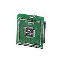
MOD PLUG-IN 44PIN PIC18LF45K22
Manufacturer
Microchip Technology
Series
PIC® XLP™ 18Fr
Datasheet
1.PIC18F26J13-ISS.pdf
(496 pages)
Specifications of MA160014
Accessory Type
Plug-In Module (PIM) - PIC18LF45K10
Product
Microcontroller Modules
Data Bus Width
8 bit
Core Processor
PIC18LF45K22
Interface Type
I2C, SPI
Operating Supply Voltage
1.8 V to 5.5 V
Lead Free Status / RoHS Status
Lead free / RoHS Compliant
For Use With/related Products
PICDEM PIC18 Explorer, DM183032
Lead Free Status / Rohs Status
Lead free / RoHS Compliant
Available stocks
Company
Part Number
Manufacturer
Quantity
Price
Company:

Part Number:
MA160014
Manufacturer:
Microchip Technology
Quantity:
135
Company:
Part Number:
MA160014
Manufacturer:
MICROCHIP
Quantity:
12 000


6.0
The Flash program memory is readable, writable and
erasable during normal operation over the entire V
range.
A read from program memory is executed one byte at
a time. A write to program memory is executed on
blocks of 64 bytes at a time. Program memory is
erased in blocks of 64 bytes at a time. The difference
between the write and erase block sizes requires from
1 to 8 block writes to restore the contents of a single
block erase. A bulk erase operation can not be issued
from user code.
Writing or erasing program memory will cease
instruction fetches until the operation is complete. The
program memory cannot be accessed during the write
or erase, therefore, code cannot execute. An internal
programming timer terminates program memory writes
and erases.
A value written to program memory does not need to be
a valid instruction. Executing a program memory
location that forms an invalid instruction results in a
NOP.
FIGURE 6-1:
2010 Microchip Technology Inc.
Note 1: Table Pointer register points to a byte in program memory.
TBLPTRU
FLASH PROGRAM MEMORY
Table Pointer
TBLPTRH
TABLE READ OPERATION
(1)
TBLPTRL
Program Memory
(TBLPTR)
Preliminary
DD
Instruction: TBLRD*
Program Memory
6.1
In order to read and write program memory, there are
two operations that allow the processor to move bytes
between the program memory space and the data RAM:
• Table Read (TBLRD)
• Table Write (TBLWT)
The program memory space is 16 bits wide, while the
data RAM space is 8 bits wide. Table reads and table
writes move data between these two memory spaces
through an 8-bit register (TABLAT).
The table read operation retrieves one byte of data
directly from program memory and places it into the
TABLAT register.
table read.
The table write operation stores one byte of data from the
TABLAT register into a write block holding register. The
procedure to write the contents of the holding registers
into program memory is detailed in
to Flash Program
operation of a table write with program memory and data
RAM.
Table operations work with byte entities. Tables
containing data, rather than program instructions, are
not required to be word aligned. Therefore, a table can
start and end at any byte address. If a table write is being
used to write executable code into program memory,
program instructions will need to be word aligned.
PIC18(L)F2X/4XK22
Table Reads and Table Writes
Figure 6-1
Memory”.
shows the operation of a
Table Latch (8-bit)
Figure 6-2
Section 6.5 “Writing
TABLAT
DS41412D-page 95
shows the
Related parts for MA160014
Image
Part Number
Description
Manufacturer
Datasheet
Request
R

Part Number:
Description:
Manufacturer:
Microchip Technology Inc.
Datasheet:
Part Number:
Description:
Manufacturer:
Microchip Technology Inc.
Datasheet:
Part Number:
Description:
Manufacturer:
Microchip Technology Inc.
Datasheet:
Part Number:
Description:
Manufacturer:
Microchip Technology Inc.
Datasheet:
Part Number:
Description:
Manufacturer:
Microchip Technology Inc.
Datasheet:
Part Number:
Description:
Manufacturer:
Microchip Technology Inc.
Datasheet:
Part Number:
Description:
Manufacturer:
Microchip Technology Inc.
Datasheet:
Part Number:
Description:
Manufacturer:
Microchip Technology Inc.
Datasheet: