EA-EDU-009 Embedded Artists, EA-EDU-009 Datasheet - Page 19
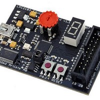
EA-EDU-009
Manufacturer Part Number
EA-EDU-009
Description
MCU, MPU & DSP Development Tools LPC2103 EDUCATION BRD
Manufacturer
Embedded Artists
Specifications of EA-EDU-009
Processor To Be Evaluated
LPC2103
Data Bus Width
16 bit, 32 bit
Interface Type
I2C, SPI, UART
Core
ARM7TDMI-S
Dimensions
68 mm x 42 mm
Maximum Operating Temperature
+ 85 C
Operating Supply Voltage
3.3 V
Lead Free Status / RoHS Status
Lead free / RoHS Compliant


NXP Semiconductors
LPC2101_02_03_4
Product data sheet
CAUTION
6.17.4 Code security (Code Read Protection - CRP)
6.17.5 External interrupt inputs
6.17.6 Memory mapping control
6.17.7 Power control
This feature of the LPC2101/02/03 allows user to enable different levels of security in the
system so that access to the on-chip flash and use of the JTAG and ISP can be restricted.
When needed, CRP is invoked by programming a specific pattern into a dedicated flash
location. IAP commands are not affected by the CRP.
Implemented in bootloader code version 2.21 are three levels of the Code Read
Protection:
Remark: Parts LPC2101/02/03 Revision ‘-’ have CRP2 enabled only (bootloader code
version 2.2).
The LPC2101/02/03 include up to three edge or level sensitive external interrupt inputs as
selectable pin functions. When the pins are combined, external events can be processed
as three independent interrupt signals. The external interrupt inputs can optionally be
used to wake-up the processor from Power-down mode and Deep power-down mode.
Additionally all 10 capture input pins can also be used as external interrupts without the
option to wake the device up from Power-down mode.
The memory mapping control alters the mapping of the interrupt vectors that appear
beginning at address 0x0000 0000. Vectors may be mapped to the bottom of the on-chip
flash memory, or to the on-chip static RAM. This allows code running in different memory
spaces to have control of the interrupts.
The LPC2101/02/03 supports three reduced power modes: Idle mode, Power-down
mode, and Deep power-down mode.
1. CRP1 disables access to chip via the JTAG and allows partial flash update (excluding
2. CRP2 disables access to chip via the JTAG and only allows full flash erase and
3. Running an application with level CRP3 selected fully disables any access to chip via
flash sector 0) using a limited set of the ISP commands. This mode is useful when
CRP is required and flash field updates are needed but all sectors cannot be erased.
update using a reduced set of the ISP commands.
the JTAG pins and the ISP. This mode effectively disables ISP override using P0.14
pin, too. It is up to the user’s application to provide (if needed) flash update
mechanism using IAP calls or call reinvoke ISP command to enable flash update via
UART0.
If level three Code Read Protection (CRP3) is selected, no future factory testing can be
performed on the device.
Rev. 04 — 2 June 2009
Single-chip 16-bit/32-bit microcontrollers
LPC2101/02/03
© NXP B.V. 2009. All rights reserved.
19 of 37
Related parts for EA-EDU-009
Image
Part Number
Description
Manufacturer
Datasheet
Request
R

Part Number:
Description:
MCU, MPU & DSP Development Tools LPC2148 EDUCATION BRD
Manufacturer:
Embedded Artists
Datasheet:

Part Number:
Description:
MCU, MPU & DSP Development Tools LPC2138 EDUCATION BRD
Manufacturer:
Embedded Artists
Datasheet:

Part Number:
Description:
MCU, MPU & DSP Development Tools EXPERIMENT EXPANSION BRD
Manufacturer:
Embedded Artists
Datasheet:

Part Number:
Description:
HEATSINK FOR TO-220 BLACK
Manufacturer:
Ohmite
Datasheet:

Part Number:
Description:
HEATSINK FOR TO-220 BLACK
Manufacturer:
Ohmite
Datasheet:

Part Number:
Description:
HEATSINK FOR TO-220 BLACK
Manufacturer:
Ohmite
Datasheet:

Part Number:
Description:
LCD Graphic Display Modules & Accessories Pure Green Backlight For DOG-M Series
Manufacturer:
ELECTRONIC ASSEMBLY
Datasheet:

Part Number:
Description:
LCD Graphic Display Modules & Accessories Grn LED Backlight For DOG-XL Series
Manufacturer:
ELECTRONIC ASSEMBLY
Datasheet:
Part Number:
Description:
LCD Graphic Display Modules & Accessories Green LED Backlight For DOG-L Series
Manufacturer:
ELECTRONIC ASSEMBLY
Datasheet:

Part Number:
Description:
KIT LPC3141 SODIMM 66X48 200POS
Manufacturer:
Embedded Artists
Datasheet:
Part Number:
Description:
KIT LPC3152 SODIMM 66X48 200POS
Manufacturer:
Embedded Artists
Datasheet:
Part Number:
Description:
BOARD OEM W/LPC2478 MCU
Manufacturer:
Embedded Artists
Datasheet:
Part Number:
Description:
KIT LPC3250 259 WITH QVGA
Manufacturer:
Embedded Artists
Datasheet: