EA-EDU-009 Embedded Artists, EA-EDU-009 Datasheet - Page 9
EA-EDU-009
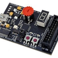
Manufacturer Part Number
EA-EDU-009
Description
MCU, MPU & DSP Development Tools LPC2103 EDUCATION BRD
Manufacturer
Embedded Artists
Specifications of EA-EDU-009
Processor To Be Evaluated
LPC2103
Data Bus Width
16 bit, 32 bit
Interface Type
I2C, SPI, UART
Core
ARM7TDMI-S
Dimensions
68 mm x 42 mm
Maximum Operating Temperature
+ 85 C
Operating Supply Voltage
3.3 V
Lead Free Status / RoHS Status
Lead free / RoHS Compliant


NXP Semiconductors
Table 3.
[1]
[2]
[3]
[4]
[5]
[6]
[7]
[8]
[9]
LPC2101_02_03_4
Product data sheet
Symbol
V
V
V
V
V
VBAT
SS
SSA
DDA
DD(1V8)
DD(3V3)
5 V tolerant (if V
Open-drain 5 V tolerant (if V
pull-up to provide an output functionality. Open-drain configuration applies to ALL functions on that pin.
5 V tolerant (if V
analog input function. If configured for an input function, this pad utilizes built-in glitch filter that blocks pulses shorter than 3 ns. When
configured as an ADC input, digital section of the pad is disabled.
5 V tolerant (if V
If configured for an input function, this pad utilizes built-in glitch filter that blocks pulses shorter than 3 ns.
A LOW level during reset on pin P0.14 is considered as an external hardware request to start the ISP command handler.
Open-drain 5 V tolerant (if V
pull-up to provide an output functionality. Open-drain configuration applies only to I
Pad provides special analog functionality.
For lowest power consumption, pin should be left floating when the RTC is not used.
See LPC2101/02/03 User manual UM10161 for details.
Pin description
Pin
7, 19, 43
31
42
5
17, 40
4
DD(3V3)
DD(3V3)
DD(3V3)
and V
and V
and V
…continued
DD(3V3)
DD(3V3)
DDA
DDA
DDA
Type
I
I
I
I
I
I
3.0 V) pad providing digital I/O functions with TTL levels and hysteresis and 10 ns slew rate control.
3.0 V) pad providing digital I/O functions with TTL levels and hysteresis and 10 ns slew rate control.
and V
3.0 V) pad providing digital I/O (with TTL levels and hysteresis and 10 ns slew rate control) and
and V
DDA
DDA
Description
Ground: 0 V reference.
Analog ground: 0 V reference. This should be nominally the same voltage as
V
Analog 3.3 V power supply: This should be nominally the same voltage as
V
pin also provides a voltage reference level for the ADC.
1.8 V core power supply: This is the power supply voltage for internal
circuitry and the on-chip PLL.
3.3 V pad power supply: This is the power supply voltage for the I/O ports.
RTC power supply: 3.3 V on this pin supplies the power to the RTC.
3.0 V) digital I/O I
3.0 V) digital I/O I
SS
DD(3V3)
but should be isolated to minimize noise and error.
Rev. 04 — 2 June 2009
but should be isolated to minimize noise and error. The level on this
2
2
C-bus 400 kHz specification compatible pad. It requires external
C-bus 400 kHz specification compatible pad. It requires external
Single-chip 16-bit/32-bit microcontrollers
2
C function on that pin.
LPC2101/02/03
© NXP B.V. 2009. All rights reserved.
9 of 37
Related parts for EA-EDU-009
Image
Part Number
Description
Manufacturer
Datasheet
Request
R

Part Number:
Description:
MCU, MPU & DSP Development Tools LPC2148 EDUCATION BRD
Manufacturer:
Embedded Artists
Datasheet:

Part Number:
Description:
MCU, MPU & DSP Development Tools LPC2138 EDUCATION BRD
Manufacturer:
Embedded Artists
Datasheet:

Part Number:
Description:
MCU, MPU & DSP Development Tools EXPERIMENT EXPANSION BRD
Manufacturer:
Embedded Artists
Datasheet:

Part Number:
Description:
HEATSINK FOR TO-220 BLACK
Manufacturer:
Ohmite
Datasheet:

Part Number:
Description:
HEATSINK FOR TO-220 BLACK
Manufacturer:
Ohmite
Datasheet:

Part Number:
Description:
HEATSINK FOR TO-220 BLACK
Manufacturer:
Ohmite
Datasheet:

Part Number:
Description:
LCD Graphic Display Modules & Accessories Pure Green Backlight For DOG-M Series
Manufacturer:
ELECTRONIC ASSEMBLY
Datasheet:

Part Number:
Description:
LCD Graphic Display Modules & Accessories Grn LED Backlight For DOG-XL Series
Manufacturer:
ELECTRONIC ASSEMBLY
Datasheet:
Part Number:
Description:
LCD Graphic Display Modules & Accessories Green LED Backlight For DOG-L Series
Manufacturer:
ELECTRONIC ASSEMBLY
Datasheet:

Part Number:
Description:
KIT LPC3141 SODIMM 66X48 200POS
Manufacturer:
Embedded Artists
Datasheet:
Part Number:
Description:
KIT LPC3152 SODIMM 66X48 200POS
Manufacturer:
Embedded Artists
Datasheet:
Part Number:
Description:
BOARD OEM W/LPC2478 MCU
Manufacturer:
Embedded Artists
Datasheet:
Part Number:
Description:
KIT LPC3250 259 WITH QVGA
Manufacturer:
Embedded Artists
Datasheet: