EA-EDU-009 Embedded Artists, EA-EDU-009 Datasheet - Page 25
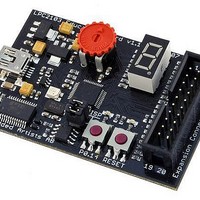
EA-EDU-009
Manufacturer Part Number
EA-EDU-009
Description
MCU, MPU & DSP Development Tools LPC2103 EDUCATION BRD
Manufacturer
Embedded Artists
Specifications of EA-EDU-009
Processor To Be Evaluated
LPC2103
Data Bus Width
16 bit, 32 bit
Interface Type
I2C, SPI, UART
Core
ARM7TDMI-S
Dimensions
68 mm x 42 mm
Maximum Operating Temperature
+ 85 C
Operating Supply Voltage
3.3 V
Lead Free Status / RoHS Status
Lead free / RoHS Compliant


NXP Semiconductors
Table 5.
T
[1]
[2]
[3]
[4]
[5]
[6]
[7]
[8]
[9]
[10] Accounts for 100 mV voltage drop in all supply lines.
[11] Allowed as long as the current limit does not exceed the maximum current allowed by the device.
[12] Minimum condition for V
[13] Applies to P0.25:16.
[14] Battery supply current on pin VBAT.
[15] Input leakage current to V
Table 6.
V
[1]
[2]
[3]
[4]
[5]
[6]
[7]
LPC2101_02_03_4
Product data sheet
Symbol
V
V
V
Symbol
V
C
E
E
E
E
E
amb
DDA
o(XTAL2)
i(RTCX1)
o(RTCX2)
IA
D
L(adj)
O
G
T
ia
Typical ratings are not guaranteed. The values listed are at room temperature (25 C), nominal supply voltages.
Core and internal rail.
External rail.
If V
If V
The RTC typically fails when V
Including voltage on outputs in 3-state mode.
V
3-state outputs go into 3-state mode when V
Conditions: V
resolution at full speed.
The ADC is monotonic, there are no missing codes.
The differential linearity error (E
The integral non-linearity (E
appropriate adjustment of gain and offset errors. See
The offset error (E
ideal curve. See
The gain error (E
error, and the straight line which fits the ideal transfer curve. See
The absolute error (E
and the ideal transfer curve. See
= 40 C to +85 C for commercial applications, unless otherwise specified.
= 2.5 V to 3.6 V; T
DD(3V3)
DD(3V3)
DDA
< 3.0 V, the I/O pins are not 5 V tolerant.
Parameter
output voltage on
pin XTAL2
input voltage on pin
RTCX1
output voltage on
pin RTCX2
Static characteristics
ADC static characteristics
supply voltages must be present.
< 3.0 V, the I/O pins are not 5 V tolerant, and the ADC input voltage is limited to V
Parameter
analog input voltage
analog input capacitance
differential linearity error
integral non-linearity
offset error
gain error
absolute error
SSA
Figure
G
= 0 V, V
O
) is the relative difference in percent between the straight line fitting the actual transfer curve after removing offset
) is the absolute difference between the straight line which fits the actual curve and the straight line which fits the
T
amb
) is the maximum difference between the center of the steps of the actual transfer curve of the non-calibrated ADC
5.
I
= 4.5 V, maximum condition for V
DDA
SS
= 40 C to +85 C unless otherwise specified. ADC frequency 4.5 MHz.
L(adj)
.
= 3.3 V and V
i(VBAT)
D
) is the peak difference between the center of the steps of the actual and the ideal transfer curve after
Conditions
) is the difference between the actual step width and the ideal step width. See
Figure
…continued
drops below 1.6 V.
5.
DD(3V3)
DD(3V3)
Conditions
= 3.3 V for 10-bit resolution at full speed; V
is grounded.
Rev. 04 — 2 June 2009
Figure
I
= 5.5 V. V
5.
Figure
DDA
5.
[1][2][3]
3.0 V and V
[1][4]
[1][5]
[1][6]
[1][7]
Single-chip 16-bit/32-bit microcontrollers
Min
0
0
0
Min
0
-
-
-
-
-
-
DD(3V3)
DDA
DDA
LPC2101/02/03
= 3.0 V.
3.0 V.
Typ
-
-
-
-
-
-
-
= 2.6 V, V
Typ
-
-
-
[1]
DD(3V3)
Figure
Max
V
1
© NXP B.V. 2009. All rights reserved.
1
2
3
0.5
4
DDA
Max
1.8
1.8
1.8
= 2.6 V for 8-bit
5.
Unit
V
pF
LSB
LSB
LSB
%
LSB
25 of 37
Unit
V
V
V
Related parts for EA-EDU-009
Image
Part Number
Description
Manufacturer
Datasheet
Request
R

Part Number:
Description:
MCU, MPU & DSP Development Tools LPC2148 EDUCATION BRD
Manufacturer:
Embedded Artists
Datasheet:

Part Number:
Description:
MCU, MPU & DSP Development Tools LPC2138 EDUCATION BRD
Manufacturer:
Embedded Artists
Datasheet:

Part Number:
Description:
MCU, MPU & DSP Development Tools EXPERIMENT EXPANSION BRD
Manufacturer:
Embedded Artists
Datasheet:

Part Number:
Description:
HEATSINK FOR TO-220 BLACK
Manufacturer:
Ohmite
Datasheet:

Part Number:
Description:
HEATSINK FOR TO-220 BLACK
Manufacturer:
Ohmite
Datasheet:

Part Number:
Description:
HEATSINK FOR TO-220 BLACK
Manufacturer:
Ohmite
Datasheet:

Part Number:
Description:
LCD Graphic Display Modules & Accessories Pure Green Backlight For DOG-M Series
Manufacturer:
ELECTRONIC ASSEMBLY
Datasheet:

Part Number:
Description:
LCD Graphic Display Modules & Accessories Grn LED Backlight For DOG-XL Series
Manufacturer:
ELECTRONIC ASSEMBLY
Datasheet:
Part Number:
Description:
LCD Graphic Display Modules & Accessories Green LED Backlight For DOG-L Series
Manufacturer:
ELECTRONIC ASSEMBLY
Datasheet:

Part Number:
Description:
KIT LPC3141 SODIMM 66X48 200POS
Manufacturer:
Embedded Artists
Datasheet:
Part Number:
Description:
KIT LPC3152 SODIMM 66X48 200POS
Manufacturer:
Embedded Artists
Datasheet:
Part Number:
Description:
BOARD OEM W/LPC2478 MCU
Manufacturer:
Embedded Artists
Datasheet:
Part Number:
Description:
KIT LPC3250 259 WITH QVGA
Manufacturer:
Embedded Artists
Datasheet: