EA-EDU-009 Embedded Artists, EA-EDU-009 Datasheet - Page 8
EA-EDU-009
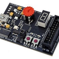
Manufacturer Part Number
EA-EDU-009
Description
MCU, MPU & DSP Development Tools LPC2103 EDUCATION BRD
Manufacturer
Embedded Artists
Specifications of EA-EDU-009
Processor To Be Evaluated
LPC2103
Data Bus Width
16 bit, 32 bit
Interface Type
I2C, SPI, UART
Core
ARM7TDMI-S
Dimensions
68 mm x 42 mm
Maximum Operating Temperature
+ 85 C
Operating Supply Voltage
3.3 V
Lead Free Status / RoHS Status
Lead free / RoHS Compliant


NXP Semiconductors
Table 3.
LPC2101_02_03_4
Product data sheet
Symbol
P0.22/AD0.0
P0.23/AD0.1
P0.24/AD0.2
P0.25/AD0.6
P0.26/AD0.7
P0.27/TRST/
CAP2.0
P0.28/TMS/
CAP2.1
P0.29/TCK/
CAP2.2
P0.30/TDI/
MAT3.3
P0.31/TDO
RTCX1
RTCX2
RTCK
XTAL1
XTAL2
DBGSEL
RST
Pin description
Pin
32
33
34
38
39
8
9
10
15
16
20
25
26
11
12
27
6
[1]
[1]
[3]
[3]
[3]
[3]
[3]
[1]
[1]
[1]
[7][8]
[7][8]
[7]
…continued
Type
I/O
I
I/O
I
I/O
I
I/O
I
I/O
I
I/O
I
I
I/O
I
I
I/O
I
I
I/O
I
O
O
O
I
O
I/O
I
O
I
I
Description
P0.22 — General purpose input/output digital pin.
AD0.0 — ADC 0, input 0.
P0.23 — General purpose input/output digital pin.
AD0.1 — ADC 0, input 1.
P0.24 — General purpose input/output digital pin.
AD0.2 — ADC 0, input 2.
P0.25 — General purpose input/output digital pin.
AD0.6 — ADC 0, input 6.
P0.26 — General purpose input/output digital pin.
AD0.7 — ADC 0, input 7.
P0.27 — General purpose input/output digital pin.
TRST — Test Reset for JTAG interface. If DBGSEL is HIGH, this pin is
automatically configured for use with EmbeddedICE (Debug mode).
CAP2.0 — Capture input for Timer 2, channel 0.
P0.28 — General purpose input/output digital pin.
TMS — Test Mode Select for JTAG interface. If DBGSEL is HIGH, this pin is
automatically configured for use with EmbeddedICE (Debug mode).
CAP2.1 — Capture input for Timer 2, channel 1.
P0.29 — General purpose input/output digital pin.
TCK — Test Clock for JTAG interface. This clock must be slower than
CPU clock (CCLK) for the JTAG interface to operate. If DBGSEL is HIGH, this
pin is automatically configured for use with EmbeddedICE (Debug mode).
CAP2.2 — Capture input for Timer 2, channel 2.
P0.30 — General purpose input/output digital pin.
TDI — Test Data In for JTAG interface. If DBGSEL is HIGH, this pin is
automatically configured for use with EmbeddedICE (Debug mode).
MAT3.3 — PWM output 3 for Timer 3.
P0.31 — General purpose output only digital pin.
TDO — Test Data Out for JTAG interface. If DBGSEL is HIGH, this pin is
automatically configured for use with EmbeddedICE (Debug mode).
Input to the RTC oscillator circuit. Input voltage must not exceed 1.8 V.
Output from the RTC oscillator circuit.
Returned test clock output: Extra signal added to the JTAG port. Assists
debugger synchronization when processor frequency varies. Bidirectional pin
with internal pull-up.
Input to the oscillator circuit and internal clock generator circuits. Input voltage
must not exceed 1.8 V.
Output from the oscillator amplifier.
Debug select: When LOW, the part operates normally. When externally
pulled HIGH at reset, P0.27 to P0.31 are configured as JTAG port, and the
part is in Debug mode
External reset input: A LOW on this pin resets the device, causing I/O ports
and peripherals to take on their default states and processor execution to
begin at address 0. TTL with hysteresis, 5 V tolerant.
Rev. 04 — 2 June 2009
[9]
. Input with internal pull-down.
Single-chip 16-bit/32-bit microcontrollers
LPC2101/02/03
© NXP B.V. 2009. All rights reserved.
1
6
of the
8 of 37
Related parts for EA-EDU-009
Image
Part Number
Description
Manufacturer
Datasheet
Request
R

Part Number:
Description:
MCU, MPU & DSP Development Tools LPC2148 EDUCATION BRD
Manufacturer:
Embedded Artists
Datasheet:

Part Number:
Description:
MCU, MPU & DSP Development Tools LPC2138 EDUCATION BRD
Manufacturer:
Embedded Artists
Datasheet:

Part Number:
Description:
MCU, MPU & DSP Development Tools EXPERIMENT EXPANSION BRD
Manufacturer:
Embedded Artists
Datasheet:

Part Number:
Description:
HEATSINK FOR TO-220 BLACK
Manufacturer:
Ohmite
Datasheet:

Part Number:
Description:
HEATSINK FOR TO-220 BLACK
Manufacturer:
Ohmite
Datasheet:

Part Number:
Description:
HEATSINK FOR TO-220 BLACK
Manufacturer:
Ohmite
Datasheet:

Part Number:
Description:
LCD Graphic Display Modules & Accessories Pure Green Backlight For DOG-M Series
Manufacturer:
ELECTRONIC ASSEMBLY
Datasheet:

Part Number:
Description:
LCD Graphic Display Modules & Accessories Grn LED Backlight For DOG-XL Series
Manufacturer:
ELECTRONIC ASSEMBLY
Datasheet:
Part Number:
Description:
LCD Graphic Display Modules & Accessories Green LED Backlight For DOG-L Series
Manufacturer:
ELECTRONIC ASSEMBLY
Datasheet:

Part Number:
Description:
KIT LPC3141 SODIMM 66X48 200POS
Manufacturer:
Embedded Artists
Datasheet:
Part Number:
Description:
KIT LPC3152 SODIMM 66X48 200POS
Manufacturer:
Embedded Artists
Datasheet:
Part Number:
Description:
BOARD OEM W/LPC2478 MCU
Manufacturer:
Embedded Artists
Datasheet:
Part Number:
Description:
KIT LPC3250 259 WITH QVGA
Manufacturer:
Embedded Artists
Datasheet: