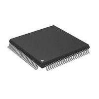
AD9398KSTZ-150 Analog Devices Inc, AD9398KSTZ-150 Datasheet - Page 13

AD9398KSTZ-150
Manufacturer Part Number
AD9398KSTZ-150
Description
IC,TV/VIDEO CIRCUIT,Video Interface Circuit,CMOS,QFP,100PIN,PLASTIC
Manufacturer
Analog Devices Inc
Datasheet
1.AD9398KSTZ-100.pdf
(44 pages)
Specifications of AD9398KSTZ-150
Applications
Video
Interface
HDMI
Voltage - Supply
3.15 V ~ 3.47 V
Package / Case
100-LQFP
Mounting Type
Surface Mount
Lead Free Status / RoHS Status
Lead free / RoHS Compliant
For Use With
AD9398/PCBZ - BOARD EVALUATION FOR AD9398
Lead Free Status / RoHS Status
Lead free / RoHS Compliant
Available stocks
Company
Part Number
Manufacturer
Quantity
Price
Company:
Part Number:
AD9398KSTZ-150
Manufacturer:
AD
Quantity:
5 510
Company:
Part Number:
AD9398KSTZ-150
Manufacturer:
AD
Quantity:
1
Company:
Part Number:
AD9398KSTZ-150
Manufacturer:
Analog Devices Inc
Quantity:
10 000
Part Number:
AD9398KSTZ-150
Manufacturer:
ADI/亚德诺
Quantity:
20 000
AUDIO BOARD LEVEL MUTING
The audio can be muted through the infoframes or locally
via the serial bus registers. This can be controlled with
Register R0x57, Bits [7:4].
AVI Infoframes
The HDMI TMDS transmission contains infoframes with
specific information for the monitor such as:
•
•
•
•
•
•
•
Table 10.
Port
Bit
4:4:4
4:2:2
4:4:4 DDR
4:2:2 to 12
1
Arrows in the table indicate clock edge. Rising edge of clock = ↑, falling edge = ↓.
•
•
•
•
•
•
Audio information
Speaker placement
N and CTS values (for reconstruction of the audio)
Muting
Source information
Video information
Vendor (transmitter source) name and product model
•
•
•
•
•
2 channels to 8 channels of audio identified
Audio coding
Audio sampling frequency
CD
SACD
DVD
Video ID code (per CEA861B)
Color space
Aspect ratio
Horizontal and vertical bar information
MPEG frame information (I, B, or P frame)
Red
7
Red/Cr [7:0]
CbCr [7:0]
DDR
DDR
CbCr [11:0]
↑
↓
6
1
R [7:0]
G [3:0]
5
4
3
DDR
↑
2
B [7:4]
1
0
Green
7
Green/Y [7:0]
DDR
DDR
Y [7:0]
Rev. 0 | Page 13 of 44
↑
↓
6
B [3:0]
G [7:4]
5
4
This information is the fundamental difference between DVI
and HDMI transmissions and is located in read-only registers
R0x5A to R0xEE. In addition to this information, registers are
provided to indicate that new information has been received.
Registers with addresses ending in 0xX7 or 0xXF beginning at
R0x87 contain the new data flag (NDF) information. These
registers contain the same information and all are reset once
any of them are read. Although there is no external interrupt
signal, it is very easy for the user to read any of these registers to
see if there is new information to be processed.
OUTPUT DATA FORMATS
The AD9398 supports 4:4:4, 4:2:2, double data rate (DDR), and
BT656 output formats. Register 0x25[3:0] controls the output
mode. These modes and the pin mapping are listed in Table 10.
3
DDR 4:2:2
DDR 4:2:2
Y [11:0]
2
↑
↓
1
CbCr [11:0]
Y,Y [11:0]
0
Blue
7
Blue/Cb [7:0]
DDR 4:2:2
6
↑
5
CbCr
4
↓
Y, Y
3
2
AD9398
1
0


