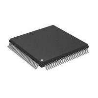
AD9398KSTZ-150 Analog Devices Inc, AD9398KSTZ-150 Datasheet - Page 25

AD9398KSTZ-150
Manufacturer Part Number
AD9398KSTZ-150
Description
IC,TV/VIDEO CIRCUIT,Video Interface Circuit,CMOS,QFP,100PIN,PLASTIC
Manufacturer
Analog Devices Inc
Datasheet
1.AD9398KSTZ-100.pdf
(44 pages)
Specifications of AD9398KSTZ-150
Applications
Video
Interface
HDMI
Voltage - Supply
3.15 V ~ 3.47 V
Package / Case
100-LQFP
Mounting Type
Surface Mount
Lead Free Status / RoHS Status
Lead free / RoHS Compliant
For Use With
AD9398/PCBZ - BOARD EVALUATION FOR AD9398
Lead Free Status / RoHS Status
Lead free / RoHS Compliant
Available stocks
Company
Part Number
Manufacturer
Quantity
Price
Company:
Part Number:
AD9398KSTZ-150
Manufacturer:
AD
Quantity:
5 510
Company:
Part Number:
AD9398KSTZ-150
Manufacturer:
AD
Quantity:
1
Company:
Part Number:
AD9398KSTZ-150
Manufacturer:
Analog Devices Inc
Quantity:
10 000
Part Number:
AD9398KSTZ-150
Manufacturer:
ADI/亚德诺
Quantity:
20 000
2-WIRE SERIAL CONTROL REGISTER DETAILS
CHIP IDENTIFICATION
0x00—Bits[7:0] Chip Revision
An 8-bit value that reflects the current chip revision.
0x11—Bit[7] HSYNC Source
0 = HSYNC, 1 = SOG. The power-up default is 0. These
selections are ignored if Register 0x11, Bit 6 = 0.
0x11—Bit[6] HSYNC Source Override
0 = auto HSYNC source, 1 = manual HSYNC source. Manual
HSYNC source is defined in Register 0x11, Bit 7. The power-up
default is 0.
0x11—Bit[5] VSYNC Source
0 = VSYNC, 1 = VSYNC from SOG. The power-up default is 0.
These selections are ignored if Register 0x11, Bit 4 = 0.
0x11—Bit[4] VSYNC Source Override
0 = auto VSYNC source, 1 = manual VSYNC source. Manual
VSYNC source is defined in Register 0x11, Bit 5. The power-up
default is 0.
0x11—Bit[3] Channel Select
0 = Channel 0, 1 = Channel 1. The power-up default is 0. These
selections are ignored if Register 0x11, Bit 2 = 0.
0x11—Bit[2] Channel Select Override
0 = auto channel select, 1 = manual channel select. Manual
channel select is defined in Register 0x11, Bit 3. The power-up
default is 0.
0x11—Bit[1] Interface Select
0 = analog interface, 1 = digital interface. The power-up default
is 0. These selections are ignored if Register 0x11, Bit 0 = 0.
0x11—Bit[0] Interface Select Override
0 = auto interface select, 1 = manual interface select. Manual
interface select is defined in Register 0x11, Bit 1. The power-up
default is 0.
0x12—Bit[7] Input HSYNC Polarity
0 = active low, 1 = active high. The power-up default is 1. These
selections are ignored if Register 10x2, Bit 6 = 0.
0x12—Bit[6] HSYNC Polarity Override
0 = auto HSYNC polarity, 1 = manual HSYNC polarity.
Manual HSYNC polarity is defined in Register 0x11, Bit 7.
The power-up default is 0.
0x12—Bit[5] Input VSYNC Polarity
0 = active low, 1 = active high. The power-up default is 1. These
selections are ignored if Register 0x11, Bit 4 = 0.
Rev. 0 | Page 25 of 44
0x12—Bit[4] VSYNC Polarity Override
0 = auto VSYNC polarity, 1 = manual VSYNC polarity. Manual
VSYNC polarity is defined in Register 0x11, Bit 5. The power-
up default is 0.
0x17—Bits[3:0] HSYNCs per VSYNC MSBs
The 4 MSBs of the 12-bit counter that reports the number of
HSYNCs/VSYNC on the active input. This is useful in
determining the mode and aid in setting the PLL divide ratio.
0x18—Bit[7:0] HSYNCs per VSYNC LSBs
The 8 LSBs of the 12-bit counter that reports the number of
HSYNCs/VSYNC on the active input.
0x21—Bit[5] VSYNC Filter Enable
The purpose of the VSYNC filter is to guarantee the position of
the VSYNC edge with respect to the HSYNC edge and to
generate a field signal. The filter works by examining the
placement of VSYNC and regenerating a correctly placed
VSYNC one line later. The VSYNC is first checked to see
whether it occurs in the Field 0 position or the Field 1 position.
This is done by checking the leading edge position against the
sync separator threshold and the HSYNC position. The HSYNC
width is divided into four quadrants with Quadrant 1 starting at
the HSYNC leading edge plus a sync separator threshold. If the
VSYNC leading edge occurs in Quadrant 1 or Quadrant 4, the
field is set to 0 and the output VSYNC is placed coincident with
the HSYNC leading edge. If the VSYNC leading edge occurs in
Quadrant 2 or Quadrant 3, the field is set to 1 and the output
VSYNC leading edge is placed in the center of the line. In this
way, the VSYNC filter creates a predictable relative position
between HSYNC and VSYNC edges at the output.
If the VSYNC occurs near the HSYNC edge, this guarantees
that the VSYNC edge follows the HSYNC edge. This performs
filtering also in that it requires a minimum of 64 lines between
VSYNCs. The VSYNC filter cleans up extraneous pulses that
might occur on the VSYNC. This should be enabled whenever
the HSYNC/VSYNC count is used. Setting this bit to 0 disables
the VSYNC filter. Setting this bit to 1 enables the VSYNC filter.
Power-up default is 0.
0x21—Bit[4] VSYNC Duration Enable
This enables the VSYNC duration block which is designed to
be used with the VSYNC filter. Setting the bit to 0 leaves the
VSYNC output duration unchanged; setting the bit to 1 sets the
VSYNC output duration based on Register 0x22. The power-up
default is 0.
0x22—Bits[7:0] VSYNC Duration
This is used to set the output duration of the VSYNC, and is
designed to be used with the VSYNC filter. This is valid only if
Register 0x21, Bit 4 is set to 1. Power-up default is 4.
AD9398


