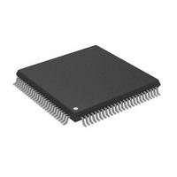
AD9398KSTZ-150 Analog Devices Inc, AD9398KSTZ-150 Datasheet - Page 26

AD9398KSTZ-150
Manufacturer Part Number
AD9398KSTZ-150
Description
IC,TV/VIDEO CIRCUIT,Video Interface Circuit,CMOS,QFP,100PIN,PLASTIC
Manufacturer
Analog Devices Inc
Datasheet
1.AD9398KSTZ-100.pdf
(44 pages)
Specifications of AD9398KSTZ-150
Applications
Video
Interface
HDMI
Voltage - Supply
3.15 V ~ 3.47 V
Package / Case
100-LQFP
Mounting Type
Surface Mount
Lead Free Status / RoHS Status
Lead free / RoHS Compliant
For Use With
AD9398/PCBZ - BOARD EVALUATION FOR AD9398
Lead Free Status / RoHS Status
Lead free / RoHS Compliant
Available stocks
Company
Part Number
Manufacturer
Quantity
Price
Company:
Part Number:
AD9398KSTZ-150
Manufacturer:
AD
Quantity:
5 510
Company:
Part Number:
AD9398KSTZ-150
Manufacturer:
AD
Quantity:
1
Company:
Part Number:
AD9398KSTZ-150
Manufacturer:
Analog Devices Inc
Quantity:
10 000
Part Number:
AD9398KSTZ-150
Manufacturer:
ADI/亚德诺
Quantity:
20 000
AD9398
0x23—Bits[7:0] HSYNC Duration
An 8-bit register that sets the duration of the HSYNC output
pulse. The leading edge of the HSYNC output is triggered by
the internally generated, phase-adjusted PLL feedback clock.
The AD9398 then counts a number of pixel clocks equal to the
value in this register. This triggers the trailing edge of the
HSYNC output, which is also phase-adjusted. The power-up
default is 32.
0x24—Bit[7] HSYNC Output Polarity
This bit sets the polarity of the HSYNC output. Setting this bit
to 0 sets the HSYNC output to active low. Setting this bit to 1
sets the HSYNC output to active high. The power-up default
setting is 1.
0x24—Bit[6] VSYNC Output Polarity
This bit sets the polarity of the VSYNC output (both DVI and
analog). Setting this bit to 0 sets the VSYNC output to active
low. Setting this bit to 1 sets the VSYNC output to active high.
Power-up default is 1.
0x24—Bit[5] Display Enable Output Polarity
This bit sets the polarity of the display enable (DE) for both
DVI and analog. 0 = DE output polarity is negative. 1 = DE
output polarity is positive. The power-up default is 1.
0x24—Bit[4] Field Output Polarity
This bit sets the polarity of the field output signal on Pin 21.
0 = active low = even field; active high = odd field. 1 = active
low = odd field; active high = even field. The power-up default
setting is 1.
0x24—Bit[0] Output Clock Invert
This bit allows inversion of the output clock as specified by
Register 0x25, Bit 7 to Bit 6. 0 = noninverted clock. 1 = inverted
clock. The power-up default setting is 0.
0x25—Bits[7:6] Output Clock Select
These bits select the clock output on the DATACLK pin. They
include ½× clock, a 2× clock, a 90° phase shifted clock, or the
normal pixel clock. The power-up default setting is 01.
Table 12. Output Clock Select
Select
00
01
10
11
Result
½× pixel clock
1× pixel clock
2× pixel clock
90° phase 1× pixel clock
Rev. 0 | Page 26 of 44
0x25—Bits[5:4] Output Drive Strength
These two bits select the drive strength for all the high speed
digital outputs (except VSOUT, A0, and O/E FIELD). Higher
drive strength results in faster rise/fall times and in general
makes it easier to capture data. Lower drive strength results in
slower rise/fall times and helps to reduce EMI and digitally
generated power supply noise. The power-up default setting is 11.
Table 13. Output Drive Strength
Output Drive
00
01
10
11
0x25—Bits[3:2] Output Mode
These bits choose between four options for the output mode,
one of which is exclusive to an HDMI input. 4:4:4 mode is
standard RGB; 4:2:2 mode is YCrCb, which reduces the number
of active output pins from 24 to 16; 4:4:4 is double data rate
(DDR) output mode; and the data is RGB mode that changes on
every clock edge. The power-up default setting is 00.
Table 14. Output Mode
Output
Mode
00
01
10
11
0x25—Bit[1] Primary Output Enable
This bit places the primary output in active or high impedance
mode. The primary output is designated when using either 4:2:2
or DDR 4:4:4. In these modes, the data on the red and green
output channels is the primary output, while the output data
on the blue channel (DDR YCrCb) is the secondary output.
0 = primary output is in high impedance mode. 1 = primary
output is enabled. The power-up default setting is 1.
0x25—Bit[0] Secondary Output Enable
This bit places the secondary output in active or high impe-
dance mode. The secondary output is designated when using
either 4:2:2 or DDR 4:4:4. In these modes, the data on the blue
output channel is the secondary output, while the output data
on the red and green channels is the primary output. Secondary
output is always a DDR YCrCb data mode. 0 = secondary
output is in high impedance mode. 1 = secondary output is
enabled. The power-up default setting is 0.
Result
4:4:4 RGB mode
4:2:2 YCrCb mode + DDR 4:2:2 on blue (secondary)
DDR 4:4:4: DDR mode + DDR 4:2:2 on blue
(secondary)
12-bit 4:2:2 (HDMI option only)
Result
Low output drive strength
Medium low output drive strength
Medium high output drive strength
High output drive strength


