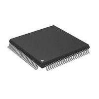
AD9398KSTZ-150 Analog Devices Inc, AD9398KSTZ-150 Datasheet - Page 15

AD9398KSTZ-150
Manufacturer Part Number
AD9398KSTZ-150
Description
IC,TV/VIDEO CIRCUIT,Video Interface Circuit,CMOS,QFP,100PIN,PLASTIC
Manufacturer
Analog Devices Inc
Datasheet
1.AD9398KSTZ-100.pdf
(44 pages)
Specifications of AD9398KSTZ-150
Applications
Video
Interface
HDMI
Voltage - Supply
3.15 V ~ 3.47 V
Package / Case
100-LQFP
Mounting Type
Surface Mount
Lead Free Status / RoHS Status
Lead free / RoHS Compliant
For Use With
AD9398/PCBZ - BOARD EVALUATION FOR AD9398
Lead Free Status / RoHS Status
Lead free / RoHS Compliant
Available stocks
Company
Part Number
Manufacturer
Quantity
Price
Company:
Part Number:
AD9398KSTZ-150
Manufacturer:
AD
Quantity:
5 510
Company:
Part Number:
AD9398KSTZ-150
Manufacturer:
AD
Quantity:
1
Company:
Part Number:
AD9398KSTZ-150
Manufacturer:
Analog Devices Inc
Quantity:
10 000
Part Number:
AD9398KSTZ-150
Manufacturer:
ADI/亚德诺
Quantity:
20 000
Hex Address
0x25
0x26
0x27
Read/Write
or Read
Only
Read/Write
Read/Write
Read/Write
Bits
[5]
[4]
[0]
[7:6]
[5:4]
[3:2]
[1]
[0]
[7]
[5]
[4]
[3]
[2:1]
[0]
[7]
[6]
[5]
Default
Value
**1*****
***1****
*******0
01******
**11****
****00**
******1*
*******0
0*******
**0*****
***0****
****1***
*****00*
*******0
1*******
*0******
**0*****
Register Name
DE Output Polarity
Field Output Polarity
Output CLK Invert
Output CLK Select
Output Drive Strength
Output Mode
Primary Output Enable
Secondary Output
Enable
Output Three-State
SPDIF Three-State
I
Power-Down Pin
Polarity
Power-Down Pin
Function
Power-Down
Auto Power-Down
Enable
HDCP A0
MCLK External Enable
2
S Three-State
Rev. 0 | Page 15 of 44
Description
Output DE polarity.
0 = active low out.
1 = active high out.
Output field polarity.
0 = active low out.
1 = active high out.
0 = don’t invert clock out.
1 = invert clock out.
Select which clock to use on output pin. 1× CLK is
divided down from TMDS clock input when pixel
repetition is in use.
00 = ½× CLK.
01 = 1× CLK.
10 = 2× CLK.
11 = 90° phase 1× CLK.
Set the drive strength of the outputs.
00 = lowest, 11 = highest.
Selects the data output mapping.
00 = 4:4:4 mode (normal).
01 = 4:2:2 + DDR 4:2:2 on blue.
10 = DDR 4:4:4 + DDR 4:2:2 on blue.
11 = 12-bit 4:2:2 (HDMI option only)
Enables primary output.
Enables secondary output (DDR 4:2:2 in Output Mode 1
and Mode 2).
Three-state the outputs.
Three-state the SPDIF output.
Three-state the I
Sets polarity of power-down pin.
0 = active low.
1 = active high.
Selects the function of the power-down pin.
00 = power-down.
01 = power-down and three-state SOG.
10 = three-state outputs only.
11 = three-state outputs and SOG.
0 = normal.
1 = power-down.
0 = disable auto low power state.
1 = enable auto low power state.
Sets the LSB of the address of the HDCP I
for a second receiver in a dual-link configuration.
0 = use internally generated MCLK.
1 = use external MCLK input.
If an external MCLK is used, it must be locked to the
video clock according to the CTS and N available in the
I
input MCLK results in dropped or repeated audio
samples.
2
C. Any mismatch between the internal MCLK and the
2
S output and the MCLK out.
2
C. Set to 1 only
AD9398


