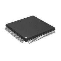
AD9398KSTZ-150 Analog Devices Inc, AD9398KSTZ-150 Datasheet - Page 14

AD9398KSTZ-150
Manufacturer Part Number
AD9398KSTZ-150
Description
IC,TV/VIDEO CIRCUIT,Video Interface Circuit,CMOS,QFP,100PIN,PLASTIC
Manufacturer
Analog Devices Inc
Datasheet
1.AD9398KSTZ-100.pdf
(44 pages)
Specifications of AD9398KSTZ-150
Applications
Video
Interface
HDMI
Voltage - Supply
3.15 V ~ 3.47 V
Package / Case
100-LQFP
Mounting Type
Surface Mount
Lead Free Status / RoHS Status
Lead free / RoHS Compliant
For Use With
AD9398/PCBZ - BOARD EVALUATION FOR AD9398
Lead Free Status / RoHS Status
Lead free / RoHS Compliant
Available stocks
Company
Part Number
Manufacturer
Quantity
Price
Company:
Part Number:
AD9398KSTZ-150
Manufacturer:
AD
Quantity:
5 510
Company:
Part Number:
AD9398KSTZ-150
Manufacturer:
AD
Quantity:
1
Company:
Part Number:
AD9398KSTZ-150
Manufacturer:
Analog Devices Inc
Quantity:
10 000
Part Number:
AD9398KSTZ-150
Manufacturer:
ADI/亚德诺
Quantity:
20 000
AD9398
2-WIRE SERIAL REGISTER MAP
The AD9398 is initialized and controlled by a set of registers that determines the operating modes. An external controller is employed to
write and read the control registers through the 2-wire serial interface port.
Table 11. Control Register Map
Hex Address
0x00
0x001
0x02
0x03
0x11
0x12
0x17
0x18
0x22
0x23
0x24
Read/Write
or Read
Only
Read
Read/Write
Read/Write
Read/Write
Read/Write
Read/Write
Read
Read
Read/Write
Read/Write
Read/Write
Bits
[7:0]
[7:0]
[7:4]
[7:6]
[5:3]
[2]
[7]
[6]
[5]
[4]
[3]
[2]
[1]
[0]
[7]
[6]
[5]
[4]
[3:0]
[7:0]
[7:0]
[7:0]
[7]
[6]
Default
Value
00000000
01101001
1101****
01******
**001***
*****0**
0*******
*0******
**0*****
***0****
****0***
*****0**
******0*
*******0
1*******
*0******
**1*****
***0****
****0000
00000000
4
32
1*******
*1******
Register Name
Chip Revision
PLL Divider MSB
PLL Divider
VCO Range
Charge Pump
PLL Enable
HSYNC Source
HSYNC Source
Override
VSYNC Source
VSYNC Source Override
Channel Select
Channel Select
Override
Interface Select
Interface Override
Input HSYNC Polarity
HSYNC Polarity
Override
Input VSYNC Polarity
VSYNC Polarity
Override
HSYNCs per VSYNC
MSB
HSYNCs per VSYNC
VSYNC Duration
HSYNC Duration
HSYNC Output Polarity
VSYNC Output Polarity
Rev. 0 | Page 14 of 44
Description
Chip revision ID. Revision is read [7:4]. [3:0].
PLL feedback divider value MSB.
PLL feedback divider value.
VCO range.
Charge pump current control for PLL.
This bit enables a lower frequency to be used for audio
MCLK generation.
0 = HSYNC.
1 = SOG.
0 = auto HSYNC source.
1 = manual HSYNC source.
0 = VSYNC.
1 = VSYNC from SOG.
0 = auto HSYNC source.
1 = manual HSYNC source.
0 = Channel 0.
1 = Channel 1.
0 = auto-channel select.
1 = manual channel select.
0 = analog interface.
1 = digital interface.
0 = auto-interface select.
1 = manual interface select.
0 = active low.
1 = active high.
0 = auto HSYNC polarity.
1 = manual HSYNC polarity.
0 = active low.
1 = active high.
0 = auto VSYNC polarity.
1 = manual VSYNC polarity.
MSB of HSYNCs per VSYNC.
HSYNCs per VSYNC count.
VSYNC duration.
HSYNC duration. Sets the duration of the output HSYNC
in pixel clocks.
Output HSYNC polarity.
0 = active low out.
1 = active high out.
0 = active low out.
1 = active high out.
Output VSYNC polarity


