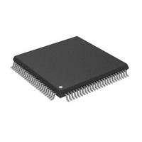
AD9398KSTZ-150 Analog Devices Inc, AD9398KSTZ-150 Datasheet - Page 27

AD9398KSTZ-150
Manufacturer Part Number
AD9398KSTZ-150
Description
IC,TV/VIDEO CIRCUIT,Video Interface Circuit,CMOS,QFP,100PIN,PLASTIC
Manufacturer
Analog Devices Inc
Datasheet
1.AD9398KSTZ-100.pdf
(44 pages)
Specifications of AD9398KSTZ-150
Applications
Video
Interface
HDMI
Voltage - Supply
3.15 V ~ 3.47 V
Package / Case
100-LQFP
Mounting Type
Surface Mount
Lead Free Status / RoHS Status
Lead free / RoHS Compliant
For Use With
AD9398/PCBZ - BOARD EVALUATION FOR AD9398
Lead Free Status / RoHS Status
Lead free / RoHS Compliant
Available stocks
Company
Part Number
Manufacturer
Quantity
Price
Company:
Part Number:
AD9398KSTZ-150
Manufacturer:
AD
Quantity:
5 510
Company:
Part Number:
AD9398KSTZ-150
Manufacturer:
AD
Quantity:
1
Company:
Part Number:
AD9398KSTZ-150
Manufacturer:
Analog Devices Inc
Quantity:
10 000
Part Number:
AD9398KSTZ-150
Manufacturer:
ADI/亚德诺
Quantity:
20 000
0x26—Bit[7] Output Three-State
When enabled, this bit puts all outputs (except SOGOUT) in a
high impedance state. 0 = normal outputs. 1 = all outputs
(except SOGOUT) in high impedance mode. The power-up
default setting is 0.
0x26—Bit[5] S/PDIF Three-State
When enabled, this bit places the S/PDIF audio output pins in a
high impedance state. 0 = normal S/PDIF output. 1 = S/PDIF
pins in high impedance mode. The power-up default setting is
0.
0x26—Bit[4] I
When enabled, this bit places the I
impedance state. 0 = normal I
impedance mode. The power-up default setting is 0.
0x26—Bit[3] Power-Down Polarity
This bit defines the polarity of the input power-down pin.
0 = power-down pin is active low. 1 = power-down pin is active
high. The power-up default setting is 1.
0x26—Bits[2:1] Power-Down Pin Function
These bits define the different operational modes of the power-
down pin. These bits are functional only when the power-down
pin is active; when it is not active, the part is powered up and
functioning. 0 = the chip is powered down and all outputs are in
high impedance mode. 1 = the chip remains powered up, but all
outputs are in high impedance mode. The power-up default
setting is 00.
0x26—Bit[0] Power-Down
This bit is used to put the chip in power-down mode. In this
mode, the power dissipation is reduced to a fraction of the
typical power (see Table 1 for exact power dissipation). When in
power-down, the HSOUT, VSOUT, DATACK, and all 30 of the
data outputs are put into a high impedance state. Note that the
SOGOUT output is not put into high impedance. Circuit blocks
that continue to be active during power-down include the
voltage references, sync processing, sync detection, and the
serial register. These blocks facilitate a fast start-up from power-
down. 0 = normal operation. 1 = power-down. The power-up
default setting is 0.
0x27—Bit[7] Auto Power-Down Enable
This bit enables the chip to go into low power mode, or seek
mode if no sync inputs are detected. 0 = auto power-down
disabled. 1 = chip powers down if no sync inputs present. The
power-up default setting is 1.
0x27—Bit[6] HDCP A0 Address
This bit sets the LSB of the address of the HDCP I
should be set to 1 only for a second receiver in a dual-link
configuration. The power-up default is 0.
2
S Three-State
2
S output. 1 = I
2
S output pins in a high
2
S pins in high
2
C. This
Rev. 0 | Page 27 of 44
0x27—Bit[5] MCLK External Enable
This bit enables the MCLK to be supplied externally. If an
external MCLK is used, then it must be locked to the video
clock according to the CTS and N available in the I
mismatch between the internal MCLK and the input MCLK
results in dropped or repeated audio samples. 0 = use internally
generated MCLK. 1 = use external MCLK input. The power-up
default setting is 0.
BT656 GENERATION
0x27—Bit[4] BT656 Enable
This bit enables the output to be BT656 compatible with the
defined start of active video (SAV) and the end of active video
(EAV) controls to be inserted. These require specification of the
number of active lines, active pixels per line, and delays to place
these markers. 0 = disable BT656 video mode. 1 = enable BT656
video mode. The power-up default setting is 0.
0x27—Bit[3] Force DE Generation
This bit allows the use of the internal DE generator in DVI
mode. 0 = internal DE generation disabled. 1 = force DE
generation via programmed registers. The power-up default
setting is 0.
0x27—Bits[2:0] Interlace Offset
These bits define the offset in HSYNCs from Field 0 to Field 1.
The power-up default setting is 000.
0x28—Bits[7:2] VSYNC Delay
These bits set the delay (in lines) from the leading edge of
VSYNC to active video. The power-up default setting is 24.
0x28—Bits[1:0] HSYNC Delay MSBs
Together with Register 0x29, these 10 bits set the delay (in
pixels) from the HSYNC leading edge to the start of active
video. The power-up default setting is 0x104.
0x29—Bits[7:0] HSYNC Delay LSBs
See the HSYNC Delay MSBs section.
0x2A—Bits[3:0] Line Width MSBs
Together with Register 0x2B, these 12 bits set the width of
the active video line (in pixels). The power-up default setting
is 0x500.
0x2B—Bits[7:0] Line Width LSBs
See the Line Width MSBs section.
0x2C—Bits[3:0] Screen Height MSBs
Along with the 8 bits following these 12 bits, set the height of
the active screen (in lines). The power-up default setting is
0x2D0.
0x2D—Bits[7:0] Screen Height LSBs
See the Screen Heights MSBs section.
2
C. Any
AD9398


