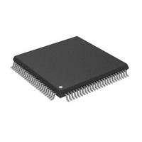
AD9398KSTZ-150 Analog Devices Inc, AD9398KSTZ-150 Datasheet - Page 8

AD9398KSTZ-150
Manufacturer Part Number
AD9398KSTZ-150
Description
IC,TV/VIDEO CIRCUIT,Video Interface Circuit,CMOS,QFP,100PIN,PLASTIC
Manufacturer
Analog Devices Inc
Datasheet
1.AD9398KSTZ-100.pdf
(44 pages)
Specifications of AD9398KSTZ-150
Applications
Video
Interface
HDMI
Voltage - Supply
3.15 V ~ 3.47 V
Package / Case
100-LQFP
Mounting Type
Surface Mount
Lead Free Status / RoHS Status
Lead free / RoHS Compliant
For Use With
AD9398/PCBZ - BOARD EVALUATION FOR AD9398
Lead Free Status / RoHS Status
Lead free / RoHS Compliant
Available stocks
Company
Part Number
Manufacturer
Quantity
Price
Company:
Part Number:
AD9398KSTZ-150
Manufacturer:
AD
Quantity:
5 510
Company:
Part Number:
AD9398KSTZ-150
Manufacturer:
AD
Quantity:
1
Company:
Part Number:
AD9398KSTZ-150
Manufacturer:
Analog Devices Inc
Quantity:
10 000
Part Number:
AD9398KSTZ-150
Manufacturer:
ADI/亚德诺
Quantity:
20 000
AD9398
Mnemonic
AUDIO DATA OUTPUT
SERIAL PORT
DATA OUTPUTS
DATA CLOCK OUTPUT
POWER SUPPLY
GND
1
The supplies should be sequenced such that V
RTERM
S/PDIF
I
MCLKIN
MCLKOUT
SCLK
LRCLK
SDA
SCL
DDCSDA
DDCSCL
MDA
MCL
RED [7:0]
GREEN [7:0]
BLUE [7:0]
DATACK
V
V
PV
DV
2
DD
S0 to I
D
DD
(3.3 V)
DD
(1.8 V
(1.8 V)
(1.8 V)
2
S3
to
3.3 V)
1
Description
RTERM is the termination resistor used to drive the AD9398 internally to a precise 50 Ω termination for TMDS lines.
This should be a 500 Ω 1% tolerance resistor.
Sony/Philips Digital Interface. Supports digital audio from 32 kbps to 192 kbps.
Inter-IC Sound Channel 0 through Channel 3. Each line supports two channels of digital audio.
Master Audio Clock External. Used if internal MCLK is not generated.
Master Audio Clock Output to Drive Audio DACs.
Serial Clock Out to support Digital Audio.
Data Output Clock for Left and Right Audio Channels.
Serial Port Data I/O for Programming AD9398 Registers—I
Serial Port Data Clock for Programming AD9398 Registers.
Serial Port Data I/O for HDCP Communications to Transmitter—I
Serial Port Data Clock for HDCP Communications to Transmitter.
Serial Port Data I/O to EEPROM with HDCP Keys—I
Serial Port Data Clock to EEPROM with HDCP Keys.
Data Output, Red Channel.
Data Output, Green Channel.
Data Output, Blue Channel.
The main data outputs. Bit 7 is the MSB. The delay from pixel sampling time to output is fixed, but is different if the
color space converter is used. When the sampling time is changed by adjusting the phase register, the output
timing is shifted as well. The DATACK and HSOUT outputs are also moved, so the timing relationship among the
signals is maintained.
Data Clock Output.
This is the main clock output signal used to strobe the output data and HSOUT into external logic. Four possible
output clocks can be selected with Register 0x25 [7:6]. These are related to the pixel clock (1/2× pixel clock,
1× pixel clock, 2× frequency pixel clock, and a 90° phase shifted pixel clock). They are produced either by the
internal PLL clock generator or EXTCLK and are synchronous with the pixel sampling clock. The polarity of DATACK
can also be inverted via Register 0x24 [0]. The sampling time of the internal pixel clock can be changed by
adjusting the phase register. When this is changed, the pixel-related DATACK timing is shifted as well. The DATA,
DATACK, and HSOUT outputs are all moved, so the timing relationship among the signals is maintained.
Analog Power Supply.
These pins supply power to the ADCs and terminators. They should be as quiet and filtered as possible.
Digital Output Power Supply.
A large number of output pins (up to 27) switching at high speed (up to 150 MHz) generates many power supply
transients (noise). These supply pins are identified separately from the V
sensitive analog circuitry can be minimized. If the AD9398 is interfacing with lower voltage logic, V
connected to a lower supply voltage (as low as 1.8 V) for compatibility.
Clock Generator Power Supply.
The most sensitive portion of the AD9398 is the clock generation circuitry. These pins provide power to the clock
PLL and help the user design for optimal performance. The designer should provide quiet, noise-free power to
these pins.
Digital Input Power Supply.
This supplies power to the digital logic.
Ground.
The ground return for all circuitry on chip. It is recommended that the AD9398 be assembled on a single solid
ground plane, with careful attention to ground current paths.
D
and V
DD
are never less than 300 mV below DV
Rev. 0 | Page 8 of 44
2
C Address is 0xA0.
DD
. At no time should DV
2
C Address is 0x98.
2
C Address is 0x74 or 0x76.
D
pins, so output noise transferred into the
DD
be more than 300 mV greater than V
DD
may be
D
or V
DD
.


