NDS9400A Fairchild Semiconductor, NDS9400A Datasheet
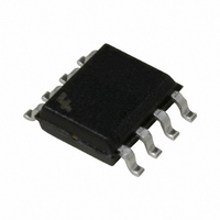
MOSFET P-CH 30V 3.4A 8-SOIC

NDS9400A

Manufacturer Part Number
NDS9400A
Description
MOSFET P-CH 30V 3.4A 8-SOIC
Manufacturer
Fairchild Semiconductor
Datasheet

Specifications of NDS9400A

Fet Type
MOSFET P-Channel, Metal Oxide
Fet Feature
Logic Level Gate
Rds On (max) @ Id, Vgs
130 mOhm @ 1A, 10V
Drain To Source Voltage (vdss)
30V
Current - Continuous Drain (id) @ 25° C
3.4A
Vgs(th) (max) @ Id
2.8V @ 250µA
Gate Charge (qg) @ Vgs
25nC @ 10V
Input Capacitance (ciss) @ Vds
350pF @ 10V
Power - Max
1W
Mounting Type
Surface Mount
Package / Case
8-SOIC (3.9mm Width)
Transistor Polarity
P Channel
Continuous Drain Current Id
2.5A
Drain Source Voltage Vds
30V
On Resistance Rds(on)
250mohm
Rds(on) Test Voltage Vgs
-10V
Threshold Voltage Vgs Typ
-1.6V
Rohs Compliant
Yes
Lead Free Status / RoHS Status
Lead free / RoHS Compliant
Other names
NDS9400ATR

Available stocks

Company
Part Number
Manufacturer
Quantity
Price
Part Number:
NDS9400A
Manufacturer:
NS
Quantity:
283
Part Number:
NDS9400A
Manufacturer:
FSC
Quantity:
350
Part Number:
NDS9400A
Manufacturer:
FSC
Quantity:
460
Part Number:
NDS9400A
Manufacturer:
FAIRCHILD/仙童
Quantity:
20 000
Absolute Maximum Ratings
________________________________________________________________________________
Symbol
V
V
I
P
T
THERMAL CHARACTERISTICS
R
R
D
© 1997 Fairchild Semiconductor Corporation
DSS
GSS
D
J
NDS9400A
Single P-Channel Enhancement Mode Field Effect Transistor
General Description
These P-Channel enhancement mode power field effect
transistors are produced using Fairchild's proprietary, high cell
density, DMOS technology. This very high density process is
especially tailored to minimize on-state resistance, provide
superior switching performance, and withstand high energy
pulses in the avalanche and commutation modes. These
devices are particularly suited for low voltage applications such
as notebook computer power management and other battery
powered circuits where fast switching, low in-line power loss,
and resistance to transients are needed.
,T
JA
JC
STG
Parameter
Drain-Source Voltage
Gate-Source Voltage
Drain Current - Continuous
Maximum Power Dissipation
Operating and Storage Temperature Range
Thermal Resistance, Junction-to-Ambient
Thermal Resistance, Junction-to-Case
- Pulsed
T
A
= 25°C unless otherwise noted
(Note 1a)
(Note 1)
(Note 1a)
(Note 1a)
(Note 1b)
(Note 1c)
Features
-3.4A, -30V. R
High density cell design for extremely low R
High power and current handling capability in a widely used
surface mount package.
Rugged and reliable.
5
6
7
8
DS(ON)
NDS9400A
-55 to 150
= 0.13
± 3.4
± 20
± 10
-30
2.5
1.2
50
25
1
@ V
GS
= -10V.
2
4
3
1
DS(ON)
February 1996
.
NDS9400A.SAM
Units
°C/W
°C/W
°C
W
V
V
A

Related parts for NDS9400A

NDS9400A Summary of contents

Page 1

... High power and current handling capability in a widely used surface mount package. Rugged and reliable 25°C unless otherwise noted A (Note 1a) (Note 1a) (Note 1b) (Note 1c) (Note 1a) (Note 1) February 1996 = 0. -10V. DS(ON DS(ON NDS9400A -30 ± 20 ± 3.4 ± 10 2.5 1.2 1 -55 to 150 50 25 NDS9400A.SAM Units °C °C/W °C/W ...

Page 2

... 125° - -1 125° -4 -0 125° - - -3 - 1.0 MHz GEN GEN Min Typ Max Units - µA -25 µA 100 nA -100 nA -1 -1.6 -2.8 V -0.85 -1.25 -2.5 0.11 0.13 0.15 0.21 0.17 0.2 0.24 0.32 - 350 pF 260 pF 100 1.6 nC 3.4 nC NDS9400A.SAM ...

Page 3

... C/W when mounted on a 0.006 in pad of 2oz cpper. 1a Scale letter size paper 2. Pulse Test: Pulse Width < 300µs, Duty Cycle < 2.0%. Conditions -1.25 A (Note -2 /dt = 100 A/µ Min Typ Max Units -1.9 -0.8 -1.3 100 1.9 is guaranteed NDS9400A.SAM ...

Page 4

... Figure 6. Gate Threshold Variation with V = -3.5V GS -4.0 -4.5 -5.0 -5 DRAIN CURRENT (A) D Voltage and Drain Current. = -10V 125°C J 25° - DRAIN CURRENT (A) D Current and Temperature -250µ 100 T , JUNCTION TEMPERATURE (°C) J Temperature. -7.0 -8.0 -10 -15 -55°C -15 GS 125 150 NDS9400A.SAM ...

Page 5

... Figure 8. Body Diode Forward Voltage iss 6 C oss rss Figure 10. Gate Charge Characteristics. 25°C 125° - 125°C J 25°C -55°C 0.4 0.6 0 BODY DIODE FORWARD VOLTAGE (V) SD Variation with Current and Temperature V = -10V = -3. GATE CHARGE (nC) g 1.4 . -20V -15V 12 NDS9400A.SAM ...

Page 6

... FR-4 Board Still Air 1 0 0.2 0 Figure 13. Maximum Steady- State Drain Current versus Copper Mounting Pad Area TIME (sec 4.5"x5" FR-4 Board Still Air 0.4 0.6 0.8 2 2oz COPPER MOUNTING PAD AREA ( ( See Note 1c JA P(pk ( Duty Cycle NDS9400A.SAM ...

Page 7

... TRADEMARKS The following are registered and unregistered trademarks Fairchild Semiconductor owns or is authorized to use and is not intended exhaustive list of all such trademarks. ACEx™ CoolFET™ CROSSVOLT™ CMOS FACT™ FACT Quiet Series™ ® FAST FASTr™ GTO™ ...

Related keywords