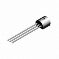
BSS100 Fairchild Semiconductor, BSS100 Datasheet - Page 2

BSS100
Manufacturer Part Number
BSS100
Description
MOSFET N-CH 100V 220MA TO92
Manufacturer
Fairchild Semiconductor
Datasheet
1.BSS123_D87Z.pdf
(5 pages)
Specifications of BSS100
Fet Type
MOSFET N-Channel, Metal Oxide
Fet Feature
Standard
Rds On (max) @ Id, Vgs
6 Ohm @ 220mA, 10V
Drain To Source Voltage (vdss)
100V
Current - Continuous Drain (id) @ 25° C
220mA
Vgs(th) (max) @ Id
2V @ 1mA
Gate Charge (qg) @ Vgs
2nC @ 10V
Input Capacitance (ciss) @ Vds
60pF @ 25V
Power - Max
630mW
Mounting Type
Through Hole
Package / Case
TO-92-3 (Standard Body), TO-226
Lead Free Status / RoHS Status
Contains lead / RoHS non-compliant
Available stocks
Company
Part Number
Manufacturer
Quantity
Price
Company:
Part Number:
BSS100
Manufacturer:
INFINEON
Quantity:
1 000
Company:
Part Number:
BSS100
Manufacturer:
FAIRCHILD
Quantity:
8 600
NOTE:
1.
Scale 1 : 1 on letter size paper
2.
Electrical Characteristics
Symbol
Off Characteristics
BV
I
I
On Characteristics
V
R
I
g
Dynamic Characteristics
C
C
C
Switching Characteristics
t
t
t
t
Q
Q
Q
Drain–Source Diode Characteristics and Maximum Ratings
I
V
t
Q
R
DSS
GSS
D(on)
d(on)
r
d(off)
f
S
rr
FS
BV
V
GS(th)
SD
DS(on)
iss
oss
rss
g
gs
gd
rr
R
the drain pins. R
Pulse Test: Pulse Width
G
GS(th)
DSS
T
T
JA
DSS
J
J
is the sum of the junction-to-case and case-to-ambient thermal resistance where the case thermal reference is defined as the solder mounting surface of
Drain–Source Breakdown Voltage
Breakdown Voltage Temperature
Coefficient
Zero Gate Voltage Drain Current
Gate–Body Leakage.
Gate Threshold Voltage
Gate Threshold Voltage
Temperature Coefficient
Static Drain–Source
On–Resistance
On–State Drain Current
Forward Transconductance
Input Capacitance
Output Capacitance
Reverse Transfer Capacitance
Gate Resistance
Turn–On Delay Time
Turn–On Rise Time
Turn–Off Delay Time
Turn–Off Fall Time
Total Gate Charge
Gate–Source Charge
Gate–Drain Charge
Maximum Continuous Drain–Source Diode Forward Current
Drain–Source Diode Forward
Voltage
Diode Reverse Recovery Time
Diode Reverse Recovery Charge
JC
is guaranteed by design while R
a) 350°C/W when mounted on a
minimum pad..
300 s, Duty Cycle
Parameter
(Note 2)
(Note 2)
2.0%
CA
is determined by the user's board design.
V
I
V
V
V
V
V
I
V
V
V
V
V
V
f = 1.0 MHz
V
V
V
V
V
V
I
d
T
D
D
F
iF
A
GS
DS
DS
DS
GS
DS
GS
GS
GS
GS
DS
DS
GS
DD
GS
DS
GS
GS
= 0.17 A,
= 250 A,Referenced to 25 C
= 1 mA,Referenced to 25 C
/d
= 25°C unless otherwise noted
= 10 V, I
= 100 V,
= 100 V,V
= 20 V,
= 20 V,
= V
= 4.5 V,
= 10V,
= 25 V,
= 30 V,
= 0 V,
= 10 V,
= 10 V,
= 15 mV, f = 1.0 MHz
= 30 V,
= 10 V,
= 10 V
= 0 V,
t
= 100 A/µs
Test Conditions
GS
,
D
GS
= 0.17 A, T
V
V
V
I
= 0 V T
I
I
I
V
I
V
I
R
I
I
GS
GS
DS
D
D
D
D
D
D
D
S
DS
GEN
GS
= 0.34 A
= 250 A
= 1 mA
= 0.17 A
= 0.17 A
= 0.17 A
= 0.28 A,
= 0.22 A,
= 0 V
= 0 V
= 0 V
= 5 V
= 0 V,
= 6
J
= 125 C
J
= 125 C
(Note 2)
Min Typ Max
0.68
0.08
100
0.8
–2.7
1.7
1.2
1.3
2.2
0.8
3.4
2.2
1.7
2.4
1.8
0.2
0.3
0.8
97
73
17
11
7
9
3
0.17
3.4
2.5
1.3
60
10
10
12
18
31
1
50
2
6
5
BSS123 Rev G(W)
Units
mV/ C
mV/ C
nC
nC
nC
nC
nA
nA
pF
pF
pF
nS
ns
ns
ns
ns
V
V
A
S
A
V
A
A


