IRF540N_R4942 Fairchild Semiconductor, IRF540N_R4942 Datasheet
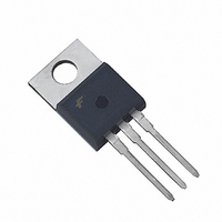
MOSFET N-CH 100V 33A TO-220AB

IRF540N_R4942

Manufacturer Part Number
IRF540N_R4942
Description
MOSFET N-CH 100V 33A TO-220AB
Manufacturer
Fairchild Semiconductor
Datasheet

Specifications of IRF540N_R4942

Fet Type
MOSFET N-Channel, Metal Oxide
Fet Feature
Standard
Rds On (max) @ Id, Vgs
40 mOhm @ 33A, 10V
Drain To Source Voltage (vdss)
100V
Current - Continuous Drain (id) @ 25° C
33A
Vgs(th) (max) @ Id
4V @ 250µA
Gate Charge (qg) @ Vgs
79nC @ 20V
Input Capacitance (ciss) @ Vds
1220pF @ 25V
Power - Max
120W
Mounting Type
Through Hole
Package / Case
TO-220-3 (Straight Leads)
Lead Free Status / RoHS Status
Contains lead / RoHS non-compliant
Other names
IRF540NFS
IRF540N_R4942
33A, 100V, 0.040 Ohm, N-Channel, Power
MOSFET
Packaging
Symbol
Absolute Maximum Ratings
Drain to Source Voltage (Note 1) . . . . . . . . . . . . . . . . . . . . . . . . . . . . . . . . . . . . . . . . . . V
Drain to Gate Voltage (R
Gate to Source Voltage . . . . . . . . . . . . . . . . . . . . . . . . . . . . . . . . . . . . . . . . . . . . . . . . . . V
Drain Current
Pulsed Avalanche Rating . . . . . . . . . . . . . . . . . . . . . . . . . . . . . . . . . . . . . . . . . . . . . . . . .UIS
Power Dissipation . . . . . . . . . . . . . . . . . . . . . . . . . . . . . . . . . . . . . . . . . . . . . . . . . . . . . . . P
Operating and Storage Temperature . . . . . . . . . . . . . . . . . . . . . . . . . . . . . . . . . . . . T
Maximum Temperature for Soldering
NOTES:
CAUTION: Stresses above those listed in “Absolute Maximum Ratings” may cause permanent damage to the device. This is a stress only rating and operation of the
device at these or any other conditions above those indicated in the operational sections of this specification is not implied.
©2002 Fairchild Semiconductor Corporation
1. T
Pulsed Drain Current . . . . . . . . . . . . . . . . . . . . . . . . . . . . . . . . . . . . . . . . . . . . . . . . . . .I
Derate Above 25
Leads at 0.063in (1.6mm) from Case for 10s. . . . . . . . . . . . . . . . . . . . . . . . . . . . . . . . . .T
Package Body for 10s, See Techbrief TB334 . . . . . . . . . . . . . . . . . . . . . . . . . . . . . . . . T
Continuous (T
Continuous (T
J
= 25
o
C to 150
C
C
o
= 25
= 100
C . . . . . . . . . . . . . . . . . . . . . . . . . . . . . . . . . . . . . . . . . . . . . . . . . . . . . . .
o
C.
JEDEC TO-220AB
GS
o
G
C, V
o
C, V
= 20k Ω ) (Note 1) . . . . . . . . . . . . . . . . . . . . . . . . . . . . . . . . V
IRF540N
GS
GS
(FLANGE)
DRAIN
= 10V) (Figure 2) . . . . . . . . . . . . . . . . . . . . . . . . . . . . . . I
D
S
= 10V) (Figure 2) . . . . . . . . . . . . . . . . . . . . . . . . . . . . . I
SOURCE
T
Data Sheet
C
DRAIN
= 25
GATE
o
C, Unless Otherwise Specified
Features
• Ultra Low On-Resistance
• Simulation Models
• Peak Current vs Pulse Width Curve
• UIS Rating Curve
Ordering Information
IRF540N
- r
- Temperature Compensated PSPICE™ and SABER
- Spice and SABER
- www.fairchildsemi.com
PART NUMBER
Electrical Models
DS(ON)
J
, T
DGR
DSS
STG
pkg
January 2002
DM
GS
D
D
D
L
= 0.040 Ω,
TO-220AB
©
V
PACKAGE
GS
Thermal Impedance Models
Figures 6, 14, 15
= 10V
-55 to 175
IRF540N
Figure 4
0.80
100
100
± 20
120
300
260
33
23
IRF540N
IRF540N
BRAND
IRF540N Rev. C
UNITS
W/
o
o
o
W
V
V
V
A
A
C
C
C
o
©
C

Related parts for IRF540N_R4942

IRF540N_R4942 Summary of contents

Page 1

... CAUTION: Stresses above those listed in “Absolute Maximum Ratings” may cause permanent damage to the device. This is a stress only rating and operation of the device at these or any other conditions above those indicated in the operational sections of this specification is not implied. ©2002 Fairchild Semiconductor Corporation January 2002 Features • ...

Page 2

... CAPACITANCE SPECIFICATIONS Input Capacitance Output Capacitance Reverse Transfer Capacitance Source to Drain Diode Specifications PARAMETER Source to Drain Diode Voltage Reverse Recovery Time Reverse Recovered Charge ©2002 Fairchild Semiconductor Corporation o C, Unless Otherwise Specified SYMBOL TEST CONDITIONS = 250 µ (Figure 11) ...

Page 3

... SINGLE PULSE 0. FIGURE 3. NORMALIZED MAXIMUM TRANSIENT THERMAL IMPEDANCE 600 100 V = 10V GS TRANSCONDUCTANCE MAY LIMIT CURRENT IN THIS REGION ©2002 Fairchild Semiconductor Corporation 150 175 125 FIGURE 2. MAXIMUM CONTINUOUS DRAIN CURRENT RECTANGULAR PULSE DURATION ( PULSE WIDTH (s) FIGURE 4. PEAK CURRENT CAPABILITY ...

Page 4

... PULSE DURATION = 80µs DUTY CYCLE = 0.5% MAX 2.5 2.0 1.5 1.0 0.5 -80 - JUNCTION TEMPERATURE ( J FIGURE 9. NORMALIZED DRAIN TO SOURCE ON RESISTANCE vs JUNCTION TEMPERATURE ©2002 Fairchild Semiconductor Corporation (Continued) SINGLE PULSE T = MAX RATED 100µs 1ms 10ms 100 300 NOTE: Refer to Application Notes AN9321 and AN9322. ...

Page 5

... FIGURE 13. GATE CHARGE WAVEFORMS FOR CONSTANT GATE CURRENT Test Circuits and Waveforms VARY t TO OBTAIN P R REQUIRED PEAK FIGURE 14. UNCLAMPED ENERGY TEST CIRCUIT ©2002 Fairchild Semiconductor Corporation (Continued) 4000 1000 80 120 160 160 200 o C) FIGURE 12. CAPACITANCE vs DRAIN TO SOURCE VOLTAGE 50V ...

Page 6

... Test Circuits and Waveforms g(REF) FIGURE 16. GATE CHARGE TEST CIRCUIT FIGURE 18. SWITCHING TIME TEST CIRCUIT ©2002 Fairchild Semiconductor Corporation (Continued DUT g(REF DUT g(TOT g(10 10V g(TH FIGURE 17. GATE CHARGE WAVEFORMS d(ON 90% 10% 50% PULSE WIDTH FIGURE 19. SWITCHING TIME WAVEFORM V = 20V ...

Page 7

... S2BMOD VSWITCH (RON = 1e-5 ROFF = 0.1 VON = 0.5 VOFF= -1.0) .ENDS NOTE: For further discussion of the PSPICE model, consult A New PSPICE Sub-Circuit for the Power MOSFET Featuring Global Temperature Options; IEEE Power Electronics Specialist Conference Records, 1991, written by William J. Hepp and C. Frank Wheatley. ©2002 Fairchild Semiconductor Corporation DPLCAP 10 RSLC2 ...

Page 8

... Fairchild Semiconductor Corporation DPLCAP 10 RSLC2 - 6 ESG 8 EVTHRES + ...

Page 9

... Fairchild Semiconductor Corporation JUNCTION th RTHERM1 CTHERM1 6 RTHERM2 CTHERM2 5 RTHERM3 CTHERM3 4 RTHERM4 CTHERM4 3 RTHERM5 ...

Page 10

... TRADEMARKS The following are registered and unregistered trademarks Fairchild Semiconductor owns or is authorized to use and is not intended exhaustive list of all such trademarks. ACEx™ FAST Bottomless™ FASTr™ FRFET™ CoolFET™ GlobalOptoisolator™ CROSSVOLT™ GTO™ DenseTrench™ ...

Related keywords