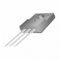
FDPF52N20T Fairchild Semiconductor, FDPF52N20T Datasheet

FDPF52N20T
Specifications of FDPF52N20T
Related parts for FDPF52N20T
FDPF52N20T Summary of contents
Page 1
... R Thermal Resistance, Case to Sink Typ. θCS R Thermal Resistance, Junction to Ambient θJA ©2007 Fairchild Semiconductor Corporation FDP52N20 / FDPF52N20T Rev. A Description = 10V 26A These N-Channel enhancement mode power field effect transis- D tors are produced using Fairchild’s proprietary, planar stripe, DMOS technology. ...
Page 2
... Starting ≤ 52A, di/dt ≤ 200A/µs, V ≤ Starting DSS 4. Pulse Test: Pulse width ≤ 300µs, Duty Cycle ≤ Essentially Independent of Operating Temperature Typical Characteristics FDP52N20 / FDPF52N20T Rev unless otherwise noted C Package Reel Size TO-220 - TO-220F - Test Conditions I = 250µ ...
Page 3
... I , Drain Current [A] D Figure 5. Capacitance Characteristics 6000 5000 C 4000 oss C iss 3000 2000 C 1000 rss Drain-Source Voltage [V] DS FDP52N20 / FDPF52N20T Rev. A Figure 2. Transfer Characteristics Notes : µ 1. 250 s Pulse Test ° Figure 4. Body Diode Forward Voltage 20V G S ° * Note : ...
Page 4
... Operation in This Area is Limited by R DS(on Drain-Source Voltage [V] DS Figure 10. Maximum Drain Current Case Temperature [ C FDP52N20 / FDPF52N20T Rev. A (Continued) Figure 8. On-Resistance Variation * Notes : µ 250 A D 100 150 200 ° Figure 9-2. Maximum Safe Operating Area 10 µ µ 100 100 ms 10 ...
Page 5
... Typical Performance Characteristics Figure 11-1. Transient Thermal Response Curve - FDP52N20 - Figure 11-2. Transient Thermal Response Curve - FDPF52N20T FDP52N20 / FDPF52N20T Rev. A (Continued) D =0.5 0.2 0.1 0.05 0.02 0.01 single pulse - are lse D uration [ D=0.5 0.2 0.1 0.05 0.02 0.01 single pulse - Square W ave Pulse Duration [sec] ...
Page 6
... FDP52N20 / FDPF52N20T Rev. A Gate Charge Test Circuit & Waveform Resistive Switching Test Circuit & Waveforms Unclamped Inductive Switching Test Circuit & Waveforms 6 www.fairchildsemi.com ...
Page 7
... FDP52N20 / FDPF52N20T Rev. A Peak Diode Recovery dv/dt Test Circuit & Waveforms + + • • • I • www.fairchildsemi.com ...
Page 8
... Mechanical Dimensions FDP52N20 / FDPF52N20T Rev 220 8 Dimensions in Millimeters www.fairchildsemi.com ...
Page 9
... Mechanical Dimensions 10.16 MAX1.47 ±0.10 0.80 ±0.10 0.35 2.54TYP ±0.20 [2.54 ] 9.40 FDP52N20 / FDPF52N20T Rev. A TO-220F ±0.20 ±0.10 ø3.18 (7.00) (1.00x45°) #1 2.54TYP ±0.20 [2.54 ] ±0.20 9 ±0.20 2.54 (0.70) +0.10 0.50 ±0.20 2.76 –0.05 Dimensions in Millimeters www.fairchildsemi.com ...
Page 10
... TRADEMARKS The following are registered and unregistered trademarks and service marks Fairchild Semiconductor owns or is authorized to use and is not intended exhaustive list of all such trademarks. ® ACEx Green FPS™ Build it Now™ Green FPS™ e-Series™ CorePLUS™ GTO™ ...


