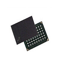
MT45W2MW16BGB-701 IT Micron Technology Inc, MT45W2MW16BGB-701 IT Datasheet - Page 17

MT45W2MW16BGB-701 IT
Manufacturer Part Number
MT45W2MW16BGB-701 IT
Description
Manufacturer
Micron Technology Inc
Datasheet
1.MT45W2MW16BGB-701_IT.pdf
(61 pages)
Specifications of MT45W2MW16BGB-701 IT
Operating Temperature (max)
85C
Operating Temperature (min)
-40C
Mounting
Surface Mount
Operating Temperature Classification
Industrial
Lead Free Status / RoHS Status
Compliant
- Current page: 17 of 61
- Download datasheet (2Mb)
Figure 11:
PDF: 09005aef82832fa2/Source: 09005aef82832f5f
32mb_burst_cr1_0_p24z_2.fm - Rev. E 9/08 EN
DQ[15:0]
LB#/UB#
A[20:0]
ADV#
WAIT
WE#
OE#
CLK
CE#
V
V
V
V
V
V
V
V
V
V
V
V
V
V
V
V
V
V
IH
IL
IH
IL
IH
IL
IH
IL
IH
IL
IH
IL
IH
IL
OH
OL
OH
OL
Refresh Collision During READ Operation
Additional WAIT states inserted to allow refresh completion
High-Z
Note:
address
Valid
ations, any disabled bytes will not be transferred to the RAM array, and the internal
value will remain unchanged. During an asynchronous WRITE cycle, the data to be
written is latched on the rising edge of CE#, WE#, LB#, or UB#, whichever occurs first.
When both the LB# and UB# are disabled (HIGH) during an operation, the device will
disable the data bus from receiving or transmitting data. Although the device will seem
to be deselected, it remains in an active mode as long as CE# remains LOW.
Nondefault BCR settings: latency code 2 (3 clocks); WAIT active LOW; WAIT asserted during
delay.
32Mb: 2 Meg x 16 Async/Page/Burst CellularRAM 1.0 Memory
17
Micron Technology, Inc., reserves the right to change products or specifications without notice.
D[0]
D[1]
Bus Operating Modes
D[2]
Undefined
©2007 Micron Technology, Inc. All rights reserved.
D[3]
Don’t Care
Related parts for MT45W2MW16BGB-701 IT
Image
Part Number
Description
Manufacturer
Datasheet
Request
R

Part Number:
Description:
IC SDRAM 64MBIT 133MHZ 54TSOP
Manufacturer:
Micron Technology Inc
Datasheet:

Part Number:
Description:
IC SDRAM 64MBIT 5.5NS 86TSOP
Manufacturer:
Micron Technology Inc
Datasheet:

Part Number:
Description:
IC SDRAM 64MBIT 200MHZ 86TSOP
Manufacturer:
Micron Technology Inc
Datasheet:

Part Number:
Description:
IC SDRAM 64MBIT 133MHZ 54TSOP
Manufacturer:
Micron Technology Inc
Datasheet:

Part Number:
Description:
IC SDRAM 128MBIT 133MHZ 54TSOP
Manufacturer:
Micron Technology Inc
Datasheet:

Part Number:
Description:
IC SDRAM 256MBIT 133MHZ 90VFBGA
Manufacturer:
Micron Technology Inc
Datasheet:

Part Number:
Description:
IC SDRAM 128MBIT 133MHZ 54TSOP
Manufacturer:
Micron Technology Inc
Datasheet:

Part Number:
Description:
IC SDRAM 256MBIT 133MHZ 54TSOP
Manufacturer:
Micron Technology Inc
Datasheet:

Part Number:
Description:
IC DDR SDRAM 512MBIT 6NS 66TSOP
Manufacturer:
Micron Technology Inc
Datasheet:

Part Number:
Description:
IC SDRAM 128MBIT 167MHZ 86TSOP
Manufacturer:
Micron Technology Inc
Datasheet:

Part Number:
Description:
IC SDRAM 128MBIT 143MHZ 86TSOP
Manufacturer:
Micron Technology Inc
Datasheet:

Part Number:
Description:
SDRAM 256M-BIT 1.8V 54-PIN VFBGA
Manufacturer:
Micron Technology Inc
Datasheet:

Part Number:
Description:
IC SDRAM 128MBIT 143MHZ 86TSOP
Manufacturer:
Micron Technology Inc
Datasheet:

Part Number:
Description:
IC SDRAM 128MBIT 125MHZ 54VFBGA
Manufacturer:
Micron Technology Inc
Datasheet:

Part Number:
Description:
IC SDRAM 128MBIT 125MHZ 54VFBGA
Manufacturer:
Micron Technology Inc
Datasheet:


