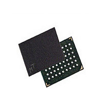
MT45W2MW16BGB-701 IT Micron Technology Inc, MT45W2MW16BGB-701 IT Datasheet - Page 6

MT45W2MW16BGB-701 IT
Manufacturer Part Number
MT45W2MW16BGB-701 IT
Description
Manufacturer
Micron Technology Inc
Datasheet
1.MT45W2MW16BGB-701_IT.pdf
(61 pages)
Specifications of MT45W2MW16BGB-701 IT
Operating Temperature (max)
85C
Operating Temperature (min)
-40C
Mounting
Surface Mount
Operating Temperature Classification
Industrial
Lead Free Status / RoHS Status
Compliant
- Current page: 6 of 61
- Download datasheet (2Mb)
Functional Block Diagram
Figure 2:
PDF: 09005aef82832fa2/Source: 09005aef82832f5f
32mb_burst_cr1_0_p24z_2.fm - Rev. E 9/08 EN
ADV#
WAIT
WE#
OE#
UB#
CLK
CRE
Functional Block Diagram – 2 Meg x 16
CE#
LB#
A[20:0]
Note:
Control
logic
Functional block diagrams illustrate simplified device operation. See ball description table,
bus operations tables, and timing diagrams for detailed information.
32Mb: 2 Meg x 16 Async/Page/Burst CellularRAM 1.0 Memory
Refresh configuration
Bus configuration
Address decode
register (RCR)
register (BCR)
logic
6
2,048K x 16
Micron Technology, Inc., reserves the right to change products or specifications without notice.
memory
DRAM
array
Functional Block Diagram
buffers
output
Input/
MUX
and
©2007 Micron Technology, Inc. All rights reserved.
DQ[7:0]
DQ[15:8]
Related parts for MT45W2MW16BGB-701 IT
Image
Part Number
Description
Manufacturer
Datasheet
Request
R

Part Number:
Description:
IC SDRAM 64MBIT 133MHZ 54TSOP
Manufacturer:
Micron Technology Inc
Datasheet:

Part Number:
Description:
IC SDRAM 64MBIT 5.5NS 86TSOP
Manufacturer:
Micron Technology Inc
Datasheet:

Part Number:
Description:
IC SDRAM 64MBIT 200MHZ 86TSOP
Manufacturer:
Micron Technology Inc
Datasheet:

Part Number:
Description:
IC SDRAM 64MBIT 133MHZ 54TSOP
Manufacturer:
Micron Technology Inc
Datasheet:

Part Number:
Description:
IC SDRAM 128MBIT 133MHZ 54TSOP
Manufacturer:
Micron Technology Inc
Datasheet:

Part Number:
Description:
IC SDRAM 256MBIT 133MHZ 90VFBGA
Manufacturer:
Micron Technology Inc
Datasheet:

Part Number:
Description:
IC SDRAM 128MBIT 133MHZ 54TSOP
Manufacturer:
Micron Technology Inc
Datasheet:

Part Number:
Description:
IC SDRAM 256MBIT 133MHZ 54TSOP
Manufacturer:
Micron Technology Inc
Datasheet:

Part Number:
Description:
IC DDR SDRAM 512MBIT 6NS 66TSOP
Manufacturer:
Micron Technology Inc
Datasheet:

Part Number:
Description:
IC SDRAM 128MBIT 167MHZ 86TSOP
Manufacturer:
Micron Technology Inc
Datasheet:

Part Number:
Description:
IC SDRAM 128MBIT 143MHZ 86TSOP
Manufacturer:
Micron Technology Inc
Datasheet:

Part Number:
Description:
SDRAM 256M-BIT 1.8V 54-PIN VFBGA
Manufacturer:
Micron Technology Inc
Datasheet:

Part Number:
Description:
IC SDRAM 128MBIT 143MHZ 86TSOP
Manufacturer:
Micron Technology Inc
Datasheet:

Part Number:
Description:
IC SDRAM 128MBIT 125MHZ 54VFBGA
Manufacturer:
Micron Technology Inc
Datasheet:

Part Number:
Description:
IC SDRAM 128MBIT 125MHZ 54VFBGA
Manufacturer:
Micron Technology Inc
Datasheet:


