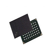
MT45W2MW16BGB-701 IT Micron Technology Inc, MT45W2MW16BGB-701 IT Datasheet - Page 21

MT45W2MW16BGB-701 IT
Manufacturer Part Number
MT45W2MW16BGB-701 IT
Description
Manufacturer
Micron Technology Inc
Datasheet
1.MT45W2MW16BGB-701_IT.pdf
(61 pages)
Specifications of MT45W2MW16BGB-701 IT
Operating Temperature (max)
85C
Operating Temperature (min)
-40C
Mounting
Surface Mount
Operating Temperature Classification
Industrial
Lead Free Status / RoHS Status
Compliant
- Current page: 21 of 61
- Download datasheet (2Mb)
Figure 14:
PDF: 09005aef82832fa2/Source: 09005aef82832f5f
32mb_burst_cr1_0_p24z_2.fm - Rev. E 9/08 EN
(except A19)
DQ[15:0]
LB#/UB#
A[20:0]
ADV#
WAIT
A19
CE#
WE#
OE#
CLK
CRE
2
3
Synchronous Mode Configuration Register WRITE Followed by READ ARRAY Operation
Latch control register value
High-Z
Notes:
t CEW
t CSP
OPCODE
t SP
t SP
t SP
t SP
1. Nondefault BCR settings for CR WRITE in synchronous mode followed by READ ARRAY
2. A[19] = LOW to load RCR, HIGH to load BCR.
3. CE# must remain LOW to complete a burst-of-one WRITE. WAIT must be monitored—addi-
t HD
t HD
t HD
t HD
operation: latency code 2 (3 clocks); WAIT active LOW; WAIT asserted during delay.
tional WAIT cycles caused by refresh collisions require a corresponding number of addi-
tional CE# LOW cycles.
32Mb: 2 Meg x 16 Async/Page/Burst CellularRAM 1.0 Memory
Latch control register address
21
Micron Technology, Inc., reserves the right to change products or specifications without notice.
t CBPH
High-Z
Address
Address
Configuration Registers
©2007 Micron Technology, Inc. All rights reserved.
Don’t Care
Valid
data
Related parts for MT45W2MW16BGB-701 IT
Image
Part Number
Description
Manufacturer
Datasheet
Request
R

Part Number:
Description:
IC SDRAM 64MBIT 133MHZ 54TSOP
Manufacturer:
Micron Technology Inc
Datasheet:

Part Number:
Description:
IC SDRAM 64MBIT 5.5NS 86TSOP
Manufacturer:
Micron Technology Inc
Datasheet:

Part Number:
Description:
IC SDRAM 64MBIT 200MHZ 86TSOP
Manufacturer:
Micron Technology Inc
Datasheet:

Part Number:
Description:
IC SDRAM 64MBIT 133MHZ 54TSOP
Manufacturer:
Micron Technology Inc
Datasheet:

Part Number:
Description:
IC SDRAM 128MBIT 133MHZ 54TSOP
Manufacturer:
Micron Technology Inc
Datasheet:

Part Number:
Description:
IC SDRAM 256MBIT 133MHZ 90VFBGA
Manufacturer:
Micron Technology Inc
Datasheet:

Part Number:
Description:
IC SDRAM 128MBIT 133MHZ 54TSOP
Manufacturer:
Micron Technology Inc
Datasheet:

Part Number:
Description:
IC SDRAM 256MBIT 133MHZ 54TSOP
Manufacturer:
Micron Technology Inc
Datasheet:

Part Number:
Description:
IC DDR SDRAM 512MBIT 6NS 66TSOP
Manufacturer:
Micron Technology Inc
Datasheet:

Part Number:
Description:
IC SDRAM 128MBIT 167MHZ 86TSOP
Manufacturer:
Micron Technology Inc
Datasheet:

Part Number:
Description:
IC SDRAM 128MBIT 143MHZ 86TSOP
Manufacturer:
Micron Technology Inc
Datasheet:

Part Number:
Description:
SDRAM 256M-BIT 1.8V 54-PIN VFBGA
Manufacturer:
Micron Technology Inc
Datasheet:

Part Number:
Description:
IC SDRAM 128MBIT 143MHZ 86TSOP
Manufacturer:
Micron Technology Inc
Datasheet:

Part Number:
Description:
IC SDRAM 128MBIT 125MHZ 54VFBGA
Manufacturer:
Micron Technology Inc
Datasheet:

Part Number:
Description:
IC SDRAM 128MBIT 125MHZ 54VFBGA
Manufacturer:
Micron Technology Inc
Datasheet:


