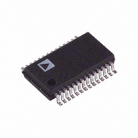
AD1871YRS Analog Devices Inc, AD1871YRS Datasheet - Page 10

AD1871YRS
Manufacturer Part Number
AD1871YRS
Description
IC ADC STEREO AUDIO 24BIT 28SSOP
Manufacturer
Analog Devices Inc
Datasheet
1.AD1871YRSZ.pdf
(28 pages)
Specifications of AD1871YRS
Rohs Status
RoHS non-compliant
Number Of Bits
24
Sampling Rate (per Second)
96k
Data Interface
Serial, SPI™
Number Of Converters
2
Voltage Supply Source
Analog and Digital
Operating Temperature
-40°C ~ 105°C
Mounting Type
Surface Mount
Package / Case
28-SSOP (0.200", 5.30mm Width)
Available stocks
Company
Part Number
Manufacturer
Quantity
Price
Company:
Part Number:
AD1871YRS
Manufacturer:
AD
Quantity:
5 510
Company:
Part Number:
AD1871YRS
Manufacturer:
PHILIPS
Quantity:
5 510
Company:
Part Number:
AD1871YRSZ
Manufacturer:
AD
Quantity:
114
Part Number:
AD1871YRSZ
Manufacturer:
ADI/亚德诺
Quantity:
20 000
AD1871
Pin
No.
1
2
3
4
5
6
7
8
9
10
11
12
13
14
15
16
17
18
19
20
21
22
23
24
25
26
27
28
NOTES
1
2
External Control Mode (See pg 11)
Modulator Mode (See pg 11)
Input/
Output
I
I
I/O
I
I
I
I
I
I
I
I
I/O
I/O
O
I
I/O
I/O
I
I
I
I
I
I
I
I/O
O
I/O
I/O
Mnemonic
MCLK
CCLK
COUT
CIN
CLATCH
DVDD
DGND
XCTRL
AVDD
VINLN
VINLP
CAPLN
CAPLP
VREF
AGND
CAPRP
CAPRN
VINRP
VINRN
AGND
CASC
DGND
ODVDD
RESET
DIN
DOUT
BCLK
LRCLK
1
2
2
1
1, 2
2
2
1
Description
Master Clock. The master clock input determines the sample rate of the device. MCLK
can be 256, 512, or 768 times the sampling frequency.
Control Port Bit Clock—clock signal for control port (SPI) interface. This pin is recon-
figured in the External Control Mode (Pin XCTRL is high), see below.
Control Port Data Out—serial data output from the control port (SPI) interface (in read-
back). This pin is reconfigured in the External Control Mode (Pin XCTRL is high), see
below; or in Modulator Mode (Bit MME of Control Register II is set), see below.
Control Port Data Input—serial data input for control port (SPI) interface. This pin is
reconfigured in the External Control Mode (Pin XCTRL is high), see below.
Control Port Frame Sync—frame sync (framing signal) for control port (SPI) interface.
This pin is reconfigured in the External Control Mode (Pin XCTRL is high), see below.
5 V Digital Core Supply
Digital Ground
External Control Enable. This pin is used to select the Control Mode for the device.
When XCTRL is low, control is via the SPI compatible control port (Pins CCLK, CLATCH,
CIN, and COUT). When XCTRL is enabled (high), control of several device functions
is possible by hardware pin strapping (Pins 256/512, M/S, DF1, and DF0). In External
Control Mode, all other functions are in default state (please refer to the Control Register
Descriptions and External Control section).
5 V Analog Supply
Left Channel, Negative Input (via MUX/PGA)
Left Channel, Positive Input (via MUX/PGA)
Left External Filter Capacitor (Negative Input to Modulator)
Left External Filter Capacitor (Positive Input to Modulator)
Reference Voltage Output. It is recommended to connect a capacitor combination of 10 mF
in parallel with 0.1 mF between VREF and AGND (Pin 15). (See Layout Recommendations.)
Analog Ground
Right External Filter Capacitor (Positive Input to Modulator)
Right External Filter Capacitor (Negative Input to Modulator)
Right Channel, Positive Input (via MUX/PGA)
Right Channel, Negative Input (via MUX/PGA)
Analog Ground
Cascade Enable. This pin enables cascading of up to four AD1871 devices to a single
DSP serial port (see Cascading section).
Digital Ground
Digital Interface Supply. The digital interface can operate from 3.3 V to 5.0 V (nominal).
Reset
Serial Data Input. Serial data input pin, only valid when the device is configured in Cas-
cade Mode (Pin CASC is high). This pin is reconfigured in Modulator Mode (Bit MME
of Control Register II is set), see below.
Audio Serial Data Output. This pin is reconfigured in Modulator Mode (Bit MME of
Control Register II is set), see below.
Audio Serial Bit Clock. The bit clock is the audio data serial clock and determines the
rate of audio data transfer. This pin is reconfigured in Modulator Mode (Bit MME of
Control Register II is set), see below.
Left/Right Clock. This clock, also known as the word clock, determines the sampling rate.
It is an output or input depending on the status of Master/Slave. This pin is reconfigured
in Modulator Mode (Bit MME of Control Register II is set), see below.
PIN FUNCTION DESCRIPTIONS
–10–
REV. 0


