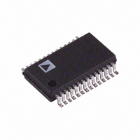
AD1871YRS Analog Devices Inc, AD1871YRS Datasheet - Page 17

AD1871YRS
Manufacturer Part Number
AD1871YRS
Description
IC ADC STEREO AUDIO 24BIT 28SSOP
Manufacturer
Analog Devices Inc
Datasheet
1.AD1871YRSZ.pdf
(28 pages)
Specifications of AD1871YRS
Rohs Status
RoHS non-compliant
Number Of Bits
24
Sampling Rate (per Second)
96k
Data Interface
Serial, SPI™
Number Of Converters
2
Voltage Supply Source
Analog and Digital
Operating Temperature
-40°C ~ 105°C
Mounting Type
Surface Mount
Package / Case
28-SSOP (0.200", 5.30mm Width)
Available stocks
Company
Part Number
Manufacturer
Quantity
Price
Company:
Part Number:
AD1871YRS
Manufacturer:
AD
Quantity:
5 510
Company:
Part Number:
AD1871YRS
Manufacturer:
PHILIPS
Quantity:
5 510
Company:
Part Number:
AD1871YRSZ
Manufacturer:
AD
Quantity:
114
Part Number:
AD1871YRSZ
Manufacturer:
ADI/亚德诺
Quantity:
20 000
Digital Decimating Filters
The filtering and decimation of the AD1871’s modulator data
stream is implemented in an embedded DSP engine. The first
stage of filtering is the sinc filtering, which has selectable deci-
mation (selected by the modulator clock control bit (AMC, see
Modulator section). The default decimation in the sinc stage
provides a sample rate reduction of 16; this corresponds with a
MODCLK rate of 128 ¥ f
Bit gives a sinc decimation factor of 8 that corresponds with a
MODCLK rate of 64 ¥ f
stage is at a rate of 8 ¥ f
The filter engine implements two half-band FIR filter sections
and a sinc compensation stage that together give a further
decimation factor of 8. Please refer to TPCs 1 through 4 for
details on the responses of the sinc and FIR filter sections.
TPC 5 gives the composite response of the sinc and FIR filters.
High-Pass Filter
The AD1871 features an optional high-pass filter section that
provides the ability of rejecting dc from the output data stream.
The high-pass filter is enabled by setting Bit 8 (HPE) of Control
Register I to 1. Please refer to TPC 7 and TPC 8 for details of
the high-pass filter characteristics.
ADC Coding
The ADC’s output data stream is in a two’s complement
encoded format. The word width can be selected from 16 bits,
20 bits, or 24 bits (see Table VI and Table VII). The coding
scheme is detailed in Table I.
Code
011111.......1111
000000........0000
100000........0001
Analog Input Section
The analog input section comprises a differential PGA stage.
It can also be configured for single-ended inputs, allowing
two such inputs to be selected via a multiplex switch. The
PGA has five gain settings (see Table V) ranging from 0 dB
to 12 dB in 3 dB steps.
In Differential Mode, the VINxP and VINxN input pins are
connected to a pair of inverting amplifiers whose outputs are
connected to the CAPxN and CAPxP pins, respectively.
(See Figure 10.)
REV. 0
Table I. ADC Coding
S
.
S
S
. The output of the sinc decimator
. The alternate setting of the AMC
Level
+Full Scale
0 (Ref Level)
–Full Scale
–17–
In Single-Ended Mode, either VINxP or VINxN can be selected
as the input. The pair of input inverting amplifiers is reconfig-
ured as a single-ended-to-differential conversion stage. Again the
outputs of the differential section are connected to Pins CAPxP
and CAPxN (see Figure 11).
The analog input section is enabled (powered ON) by default
on reset. If it is required to bypass the analog input section by
using the modulator input pins (CAPxP and CAPxN) directly,
then the analog input section must be powered down by setting
Bits MER and MEL in Control Register III.
Serial Data Interface
The AD1871’s serial data interface consists of three pins
(LRCLK, BCLK, and SDATA). LRCLK is the framing sig-
nal for left and right channel samples and its frequency is
equal to the sampling frequency (f
used to clock the data samples from the AD1871 and its fre-
quency is equal to 64 ¥ f
of the left and right channels). SDATA outputs the left and right
channel sample data coincident with the falling edge of BCLK.
The serial data interface supports all the popular audio interface
standards, such as I
well as the serial interfaces of modern DSPs. The Interface Mode is
selected by programming the Bits DF1–DF0 of Control Register II
(see Tables VI and VIII).
The data sample width can be selected from 16, 20, or 24 bits by
programming Bits WW1–WW0 of Control Register II (see
Tables VI and VII).
VINxN
VINxN
VINxP
VINxP
Figure 11. Single-Ended Analog Input
Figure 10. Differential Analog Input
2
S, left-justified (LJ), and right-justified (RJ), as
V
V
CM
CM
S
(giving 32 BCLK periods for each
S
). BCLK is the serial clock
V
V
CM
CM
AD1871
CAPxN
CAPxP
CAPxN
CAPxP


