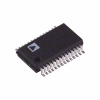
AD1871YRS Analog Devices Inc, AD1871YRS Datasheet - Page 20

AD1871YRS
Manufacturer Part Number
AD1871YRS
Description
IC ADC STEREO AUDIO 24BIT 28SSOP
Manufacturer
Analog Devices Inc
Datasheet
1.AD1871YRSZ.pdf
(28 pages)
Specifications of AD1871YRS
Rohs Status
RoHS non-compliant
Number Of Bits
24
Sampling Rate (per Second)
96k
Data Interface
Serial, SPI™
Number Of Converters
2
Voltage Supply Source
Analog and Digital
Operating Temperature
-40°C ~ 105°C
Mounting Type
Surface Mount
Package / Case
28-SSOP (0.200", 5.30mm Width)
Available stocks
Company
Part Number
Manufacturer
Quantity
Price
Company:
Part Number:
AD1871YRS
Manufacturer:
AD
Quantity:
5 510
Company:
Part Number:
AD1871YRS
Manufacturer:
PHILIPS
Quantity:
5 510
Company:
Part Number:
AD1871YRSZ
Manufacturer:
AD
Quantity:
114
Part Number:
AD1871YRSZ
Manufacturer:
ADI/亚德诺
Quantity:
20 000
AD1871
CONTROL/STATUS REGISTERS
The AD1871’s Operating Mode is set by programming three,
10-bit Control Registers via an SPI compatible port. Table III
details the format of the AD1871 control words, which are 16
bits wide with a 4-bit address field in Positions 15 through 12,
a Read/Write Bit in Position 11, a Reserved Bit in Position 10,
and 10 bits of register data (corresponding to the control regis-
ter width) in Positions 9 through 0. The three control words
occupy Addresses 0000b through 0010b in the register map (see
Table II).
The AD1871 also features two readback (status) registers that
can be enabled to track the peak reading on each of the chan-
nels (left and right). These 6-bit results are read back via the
SPI compatible port in a 16-bit frame similar to that of the
control words.
LRCLK
CLAT CH
DOU T
DOU T
BCLK
BCLK
CCLK
CI N
CCLK
M SB
CI N
1
DEV I CE 1
M SB
– 1
2
DEV I CE 1
LEFT CH AN N EL
M SB
– 2
3
M SB
LSB
2 3
+1
M SB
– 1
2 4
LSB
Figure 18. Cascade Mode Data Interface Timing
Figure 19. Cascade Mode Control Port Timing
DEV I CE 2
DEV I CE 2
–20–
The SPI compatible control port features four signals (CCLK,
CLATCH, CDATA, and COUT). The CLATCH signal is an
enable line that must be low to allow communication to or from
the control port. The CCLK is the serial clock that clocks in
serial data via the CDATA pin and clocks out serial data via the
COUT pin. Figures 20 and 21 show details of the control port
timing.
M SB
1
DEV I CE 3
M SB
– 1
DEV I CE 3
2
RI GH T CH AN N EL
M SB
– 2
3
Address
0000
0001
0010
0011
0100
Table II. Register Address Map
LSB
+1
LSB
2 3
+1
LSB
2 4
LSB
Control Register
Control Register I
Control Register II
Control Register III
Peak Reading Register I
Peak Reading Register II
DEV I CE 4
DEV I CE 4
REV. 0


