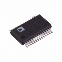
AD1871YRS Analog Devices Inc, AD1871YRS Datasheet - Page 24

AD1871YRS
Manufacturer Part Number
AD1871YRS
Description
IC ADC STEREO AUDIO 24BIT 28SSOP
Manufacturer
Analog Devices Inc
Datasheet
1.AD1871YRSZ.pdf
(28 pages)
Specifications of AD1871YRS
Rohs Status
RoHS non-compliant
Number Of Bits
24
Sampling Rate (per Second)
96k
Data Interface
Serial, SPI™
Number Of Converters
2
Voltage Supply Source
Analog and Digital
Operating Temperature
-40°C ~ 105°C
Mounting Type
Surface Mount
Package / Case
28-SSOP (0.200", 5.30mm Width)
Available stocks
Company
Part Number
Manufacturer
Quantity
Price
Company:
Part Number:
AD1871YRS
Manufacturer:
AD
Quantity:
5 510
Company:
Part Number:
AD1871YRS
Manufacturer:
PHILIPS
Quantity:
5 510
Company:
Part Number:
AD1871YRSZ
Manufacturer:
AD
Quantity:
114
Part Number:
AD1871YRSZ
Manufacturer:
ADI/亚德诺
Quantity:
20 000
AD1871
15–12
15–12
Peak Reading Registers
The Peak Reading Registers are read-only registers that can be
enabled to track-and-hold the peak ADC reading from each
channel. The peak reading feature is enabled by setting Bit PRE
in Control Register I. The peak reading value is contained in the
six LSBs of the 10-bit readback word. The result is binary coded
where each LSB is equivalent to –1 dBFS with all zeros cor-
responding to full scale (0 dBFS) and all ones corresponding
to –63 dBFS (see Table XVI). When Bit PRE is set, the peak
reading per channel is stored in the appropriate peak register.
Once the register is read, the register value is set to zero and is
updated by subsequent conversions.
AxP
A Peak Reading Register read cycle is detailed in Figure 21.
EXTERNAL CONTROL
The AD1871 can be configured for external hardware control of
a subset of the device functionality. This functionality includes
Master/Slave Mode select, MCLK select, and serial data
format select. External control is enabled by tying the XCTRL
Pin high as shown in Figure 22.
0011
0100
Figure 22. External Control Configuration
5 4 3 2 1 0
0 0 0 0 0 0
0 0 0 0 0 1
0 0 0 0 1 0
1 1 1 1 1 0
1 1 1 1 1 1
Table XVI. Peak Reading Result Format
11
11
1
1
Code
10
9–6
5–0
10
9–6
5–0
AD1871
0
0
Reserved
A0P5–A0P0
9
9
Reserved
A1P5–A1P0
XCTRL
Table XIV. Peak Reading Register I (Address 0011b, Read-Only)
Table XV. Peak Reading Register II (Address 0100b, Read-Only)
V
DD
8
8
Level
0 dBFS
–1 dBFS
–2 dBFS
–62 dBFS
–63 dBFS
(Always Set to Zero)
Left Channel Peak Reading (Valid Only When PRE = 1)
(Always Set to Zero)
Right Channel Peak Reading (Valid Only When PRE = 1)
7
7
6
6
–24–
Master/Slave Select
The Master/Slave hardware select (Pin 5, CLATCH/[M/S])
is equivalent to setting the M/S Bit of Control Register II. If set
low, the device is placed in Master Mode, whereby the LRCLK
and BCLK signals are outputs from the AD1871.
When M/S is set high, the device is in Slave Mode, whereby the
LRCK and BCLK signals are inputs to the AD1871.
MCLK Mode Select
The MCLK Mode hardware select (Pin 2, CCLK/[256/512]) is
a subset of the MCLK Mode selection that is determined by
Bits CM1–CM0 of Control Register X. When the hardware pin
is low, the device operates with an MCLK that is 256 ¥ f
pin is set high, the device operates with an MCLK that is 512 ¥ f
Serial Data Format Select
The Serial Data Format hardware select (Pins 3 and 4, DF0/
COUT and DF1/CIN) is equivalent to setting Bits DF1–DF0 of
Control Register II. See Table VIII.
In External Control Mode, all functions other than those
selected by the hardware select pins (Master/Slave Mode select,
MCLK select, and Serial Data Format select) are in their
default (power-on) state.
MODULATOR MODE
When the device is in Modulator Mode (MME Bit is set to 1),
the D[0–3] pins are enabled as data outputs, while the COUT
pin becomes MODCLK, a high speed sampling clock (nomi-
nally at 128
the left and right channel modulators with left channel modula-
tor data being valid in the low phase of MODCLK, while right
channel modulator data is valid under the high phase of MODCLK
(see Modulator Mode Timing in Figure 6).
The Modulator Mode is designed to be used for applications
such as direct stream digital (DSD) where modulator data is
stored directly to the recording media without decimation and
filtering to a lower sample rate. DSD is specified at a rate of
64
requiring an intermediate remodulator that downsamples to
64
A0P5
A1P5
5
5
f
f
S
S
, whereas the AD1871 outputs at 128
and generates a single-bit output steam.
A0P4
A1P4
4
4
f
S
). The MODCLK enables successive data from
A0P3
A1P3
3
3
A0P2
A1P2
2
2
A0P1
A1P1
1
1
f
S
,
A0P0
A1P0
S
REV. 0
0
0
; if the
S
.


