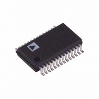
AD1871YRS Analog Devices Inc, AD1871YRS Datasheet - Page 22

AD1871YRS
Manufacturer Part Number
AD1871YRS
Description
IC ADC STEREO AUDIO 24BIT 28SSOP
Manufacturer
Analog Devices Inc
Datasheet
1.AD1871YRSZ.pdf
(28 pages)
Specifications of AD1871YRS
Rohs Status
RoHS non-compliant
Number Of Bits
24
Sampling Rate (per Second)
96k
Data Interface
Serial, SPI™
Number Of Converters
2
Voltage Supply Source
Analog and Digital
Operating Temperature
-40°C ~ 105°C
Mounting Type
Surface Mount
Package / Case
28-SSOP (0.200", 5.30mm Width)
Available stocks
Company
Part Number
Manufacturer
Quantity
Price
Company:
Part Number:
AD1871YRS
Manufacturer:
AD
Quantity:
5 510
Company:
Part Number:
AD1871YRS
Manufacturer:
PHILIPS
Quantity:
5 510
Company:
Part Number:
AD1871YRSZ
Manufacturer:
AD
Quantity:
114
Part Number:
AD1871YRSZ
Manufacturer:
ADI/亚德诺
Quantity:
20 000
AD1871
Modulator Clock
The modulator clock can be chosen to be either 128 ¥ f
64 ¥ f
clock rate. When AMC is set to 0 (default), the modulator clock
is 128 ¥ f
This bit is normally set depending on whether the desired sampling
frequency is 48 kHz or 96 kHz and is also influenced by the
selected MCLK frequency. Please refer to the Functional
Description section for more information on MCLK selection
and sampling rates.
Power-Down
Power-down of the active clock signals within the AD1871 is
effected by writing a Logic 1 to Bit 7 (PD). In Power-Down
15–12
Control Register II
Control Register II contains bit settings for control of left/right
channel muting, data sample word width, data interface format,
and direct modulator bitstream output.
Mute Control
The left and right data channels can be muted to digital zero by
setting the MUL and MUR Bits (Bits 0 and 1), respectively. If a
channel is muted, its output data stream will remain at digital
zero, regardless of the amplitude of the input signal. Setting the
bit to 1 mutes the channel while setting the bit to 0 restores
normal operation.
Master/Slave Select
The AD1871 can operate as either a slave device or a master
device. In Slave Mode, the controller must provide the LRCLK
and BCLK to determine the sample rate and serial bit rate. In
Master Mode, the AD1871 provides the LRCLK and BCLK as
outputs that are applied to the controller. The AD1871 defaults to
Master Mode (M/S is low) on reset.
Word Width
The AD1871 allows the output sample word width to be selected
from 16, 20, and 24 bits wide. Compact disc (CD) compatibility
may require 16 bits, while many modern digital audio formats
require 24-bit sample resolution. Bits WW1–WW0 are programmed
to select the word width. Table VII details the Control Register
Bit settings corresponding to the various word width selections.
0001
S
. The AMC Bit (Bit 6) is used to select the modulator’s
S
. Otherwise, if set to 1, the modulator clock is 64 ¥ f
11
0
10
0
9–8
6–5
4–3
9
7
2
1
0
MME
DF1–DF0
WW1–WW0
M/S
MUR
MUL
8
Table VI. Control Register II (Address 0001b)
MME
7
S
DF1
Reserved
Modulator Mode Enable (0 = Normal Mode (Default), 1 = Mod Mode)
Data Format (See Table VIII)
Word Width (See Table VII)
Master/Slave Select (0 = Master Mode (Default); 1 = Slave Mode)
Mute Control, Right Channel (0 = Disabled (Default); 1 = Enabled)
Mute Control, Left Channel (0 = Disabled (Default); 1 = Enabled)
or
6
S
.
–22–
Mode, digital activity is suspended and analog sections are
powered down, with the exception of the reference.
High-Pass Filter
The AD1871’s digital filtering engine allows the insertion of a
high-pass filter (HPF) to effectively block dc signals from the
output digital waveform. Setting Bit 8 (HPE) enables the
high-pass filter. For more details of the HPF, refer to the
Functional Description section.
Peak Reading Enable
The AD1871 has two readback registers that can be enabled to
store the peak readings of the left and right channel ADC results.
To enable the peak readings to be captured, the Peak Reading
Enable Bit (PRE), Bit 9, must be set to Logic 1. When set to
Logic 0, the peak reading capture is disabled.
WW1
0
0
1
1
Data Format
The AD1871’s serial data interface can be configured from a
choice of popular interface formats, including I
right-justified, or DSP Modes. Bits DF1–DF0 are programmed to
select the interface format (mode) as shown in Table VIII.
DF1
0
0
1
1
*Please refer to the Serial Data Interface section in the Functional
Modulator Mode Enable
The AD1871 defaults to the conversion of the analog audio to
linear, PCM-encoded digital outputs. Modulator Mode allows
the user to bypass the digital decimation filter section and access
the multibit sigma-delta modulator outputs directly. When in
this mode, certain pins are redefined (see Modulator Mode) and
the modulator output (at a nominal rate of 128
on the modulator data pins (D[0–3]). To enable the Modu-
lator Mode, set the MME Bit to high.
DF0
Description for more details on the various interface modes.
5
Table VIII. Data Interface Format Settings*
WW1
4
WW0
DF0
0
1
0
1
0
1
0
1
Table VII. Word-Width Settings
WW0
3
24 (Default)
20
16
Reserved
Word Width (No. of Bits)
Interface Mode
I
Right-Justified
DSP
Left-Justified
2
S (Default)
M/S
2
MUR
1
2
S, left-justified,
f
S
) is available
MUL
0
REV. 0


