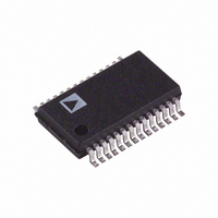
AD1871YRS Analog Devices Inc, AD1871YRS Datasheet - Page 21

AD1871YRS
Manufacturer Part Number
AD1871YRS
Description
IC ADC STEREO AUDIO 24BIT 28SSOP
Manufacturer
Analog Devices Inc
Datasheet
1.AD1871YRSZ.pdf
(28 pages)
Specifications of AD1871YRS
Rohs Status
RoHS non-compliant
Number Of Bits
24
Sampling Rate (per Second)
96k
Data Interface
Serial, SPI™
Number Of Converters
2
Voltage Supply Source
Analog and Digital
Operating Temperature
-40°C ~ 105°C
Mounting Type
Surface Mount
Package / Case
28-SSOP (0.200", 5.30mm Width)
Available stocks
Company
Part Number
Manufacturer
Quantity
Price
Company:
Part Number:
AD1871YRS
Manufacturer:
AD
Quantity:
5 510
Company:
Part Number:
AD1871YRS
Manufacturer:
PHILIPS
Quantity:
5 510
Company:
Part Number:
AD1871YRSZ
Manufacturer:
AD
Quantity:
114
Part Number:
AD1871YRSZ
Manufacturer:
ADI/亚德诺
Quantity:
20 000
Control Register I
Control Register I contains bit settings for control of analog
front end gain, modulator clock selection, power-down control,
high-pass filtering, and peak hold.
Analog Gain Control
The AD1871 features an optional analog front end with select-
able gain. Gain is selected using three control bits for each channel,
giving five separate and independent gain settings on each channel.
Bits 2 through 0 (AGR2–AGR0) set the analog gain for the right
channel, while Bits 5 through 3 (AGL2–AGL0) set the analog
gain for the left channel. Table V shows the analog gain corre-
sponding to the bit settings in AGx2–ADx0.
REV. 0
15-12
Address
15–12
0000
11
0
R/W
11
10
0
CLATCH
CLATCH
Reserved
CCLK
COUT
CCLK
COUT
CIN
CIN
PRE
10
5–3
2–0
9
9
8
7
6
D15
D15
Table IV. Control Register I (Address 0000b, Write Only)
Figure 21. Reading from Register Using Control Port
HPE
PRE
HPE
PD
AMC
AGL2–AGL0
AGR2–AGL0
Figure 20. Writing to Register Using Control Port
9
D14
D14
8
D13
D13
Table III. Control/Status Word Format
D12
D12
PD
7
6
D11
D11
D10
D10
AMC
Peak Reading Enable (0 = Disabled (Default); 1 = Enabled)
High-Pass Filter Enable (0 = Disabled (Default); 1 = Enabled)
Power-Down Control (1 = Power-Down; 0 = Normal Operation (Default))
ADC Modulator Clock (1 = 64 ¥ f
Input Gain (Left Channel, see Table V)
Input Gain (Right Channel, see Table V)
6
5
D09
D09
D09
–21–
D08
D08
D08
AGL2
AGx2
4
Control/Status Data Bits (9–0)
D07
D07
D07
5
0
0
0
0
1
1
1
1
D06
D06
D06
D05
D05
D05
AGL1
AGx1
3
4
0
0
1
1
0
0
1
1
D04
D04
D04
Table V. Analog Gain Settings
D03
D03
D03
AGx0
2
AGL0
D02
0
1
0
1
0
1
0
1
D02
D02
3
S
; 0 = 128 ¥ f
D01
D01
D01
1
D00
D00
D00
AGR2
Gain (dB)
0 (Default)
2
12
S
3
6
9
0
0
0
(Default))
0
AGR1
1
AD1871
AGR0
0


