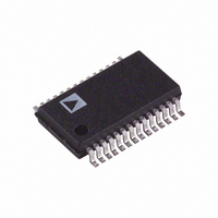
AD1871YRS Analog Devices Inc, AD1871YRS Datasheet - Page 23

AD1871YRS
Manufacturer Part Number
AD1871YRS
Description
IC ADC STEREO AUDIO 24BIT 28SSOP
Manufacturer
Analog Devices Inc
Datasheet
1.AD1871YRSZ.pdf
(28 pages)
Specifications of AD1871YRS
Rohs Status
RoHS non-compliant
Number Of Bits
24
Sampling Rate (per Second)
96k
Data Interface
Serial, SPI™
Number Of Converters
2
Voltage Supply Source
Analog and Digital
Operating Temperature
-40°C ~ 105°C
Mounting Type
Surface Mount
Package / Case
28-SSOP (0.200", 5.30mm Width)
Available stocks
Company
Part Number
Manufacturer
Quantity
Price
Company:
Part Number:
AD1871YRS
Manufacturer:
AD
Quantity:
5 510
Company:
Part Number:
AD1871YRS
Manufacturer:
PHILIPS
Quantity:
5 510
Company:
Part Number:
AD1871YRSZ
Manufacturer:
AD
Quantity:
114
Part Number:
AD1871YRSZ
Manufacturer:
ADI/亚德诺
Quantity:
20 000
15–12
0010
Control Register III
Control Register III contains bit settings for configuration of the
analog input section (both left and right channels).
Mux Enable
The Mux Enable Left (MEL) and Mux Enable Right (MER)
are used to enable the analog buffers. When these bits are set to
1, the analog input buffers are powered down and input signals
must be applied directly to the modulator inputs via the CAPxP
and CAPxN pins. (see Figure 23). When MEL and MER are set
to 0 (default condition after reset), the analog input section is
enabled, (see Table X).
MEL
Mux Select
The Mux Select Bits (MXL and MXR for left and right channels,
respectively) are used to select the input from VINxP or VINxN
when the input is configured as single-ended. When MXx is set
to 0, the input is taken from VINxP. When MXx is set to 1, the
input is taken from VINxN, (see Table XI).
MXL
*Mux select settings are only valid when single-ended operation is enabled; SEL
REV. 0
and SER are set to 1.
0
1
X
X
0
1
X
X
11
0
MER
MXR
X
X
0
1
X
X
0
1
Table XI. Mux Select Settings*
Table X. Mux Control Settings
9–8
7–6
5
4
3
2
1
0
10
0
Input Setting
Left Channel Analog Buffer Enabled
Left Channel Analog Buffer Disabled
Right Channel Analog Buffer Enabled
Right Channel Analog Buffer Disabled
Input Setting
Left Channel Input from VINLP
Left Channel Input from VINLN
Right Channel Input from VINRP
Right Channel Input from VINRN
Reserved
MCD1–MCD0 Master Clock Divider (See Table XIII)
SEL
SER
MEL
MXL
MER
MXR
9
8
Table IX. Control Register III (Address 0010b)
(Should Be Programmed to 0)
Single-Ended Enable, Left Channel (0 = Differential (Default); 1 = Single-Ended)
Single-Ended Enable, Right Channel (0 = Differential (Default); 1 = Single-Ended)
Mux/PGA Disable, Left Channel (0 = Enabled (Default); 1 = Disabled)
Mux Select, Left Channel (0 = VINLP Selected (Default); 1 = VINLN Selected)
Mux/PGA Disable, Right Channel (0 = Enabled (Default); 1 = Disabled)
Mux Select, Right Channel (0 = VINRP Selected (Default); 1 = VINRN Selected)
MCD1 MCD0
7
6
–23–
Single-Ended Mode Enable
The Single-Ended Mode Enable Bits (SEL and SER for left and
right channels, respectively), when set to 1, are used to configure
single-ended input on VINxP and VINxN (input is selected by
state of MXL and MXR). In this mode, single-ended inputs taken
from either VINxP or VINxN (selected using the Mux Select
Bits—MXL and MXR) are internally converted to a differential
format to be applied to the modulator section (see Table XII).
SEL
Master Clock Divider
The master clock divider allows the division of the external
MCLK frequency to a more suitable internal master clock
frequency (IMCLK). IMCLK must be 256 ¥ f
the available MCLK is not at 256 ¥ f
this, the MCD allows conversion of MCLK to a suitable IMCLK
at 256 ¥ f
MCD1
SEL
0
1
X
X
0
0
1
1
5
S
Table XII. Differential/Single-Ended Select
SER
Table XIII. Master Clock Divider Settings
(see Table XIII).
4
SER
MCD0
X
X
0
1
0
1
0
1
MEL
3
Input Setting
Left Channel Input Æ Differential
Left Channel Input Æ Single-Ended
Right Channel Input Æ Differential
Right Channel Input Æ Single-Ended
MCLK Division
IMCLK = MCLK (/1)
IMCLK = MCLK/2
IMCLK = MCLK/3
IMCLK = MCLK (/1)
MXL
2
S
but is a multiple of
MER
1
AD1871
S
; therefore, if
MXR
0


