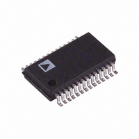
AD1871YRS Analog Devices Inc, AD1871YRS Datasheet - Page 26

AD1871YRS
Manufacturer Part Number
AD1871YRS
Description
IC ADC STEREO AUDIO 24BIT 28SSOP
Manufacturer
Analog Devices Inc
Datasheet
1.AD1871YRSZ.pdf
(28 pages)
Specifications of AD1871YRS
Rohs Status
RoHS non-compliant
Number Of Bits
24
Sampling Rate (per Second)
96k
Data Interface
Serial, SPI™
Number Of Converters
2
Voltage Supply Source
Analog and Digital
Operating Temperature
-40°C ~ 105°C
Mounting Type
Surface Mount
Package / Case
28-SSOP (0.200", 5.30mm Width)
Available stocks
Company
Part Number
Manufacturer
Quantity
Price
Company:
Part Number:
AD1871YRS
Manufacturer:
AD
Quantity:
5 510
Company:
Part Number:
AD1871YRS
Manufacturer:
PHILIPS
Quantity:
5 510
Company:
Part Number:
AD1871YRSZ
Manufacturer:
AD
Quantity:
114
Part Number:
AD1871YRSZ
Manufacturer:
ADI/亚德诺
Quantity:
20 000
AD1871
LAYOUT CONSIDERATIONS
In order to operate the AD1871 at its specified performance level,
careful consideration must be given to the layout of the AD1871
and its ancillary circuits. Since the analog inputs to the AD1871
are differential, the voltages in the analog modulator are common-
mode voltages. The excellent common-mode rejection of the part
will remove common-mode noise on these inputs. The analog
and digital supplies of the AD1871 are independent and sepa-
rately pinned out to minimize coupling between the analog and
digital sections of the device. The digital filters will provide
rejection of broadband noise on the power supplies, except at
integer multiples of the modulator sampling frequency. The
digital filters also remove noise from the analog inputs provided
the noise source does not saturate the analog modulator.
However, because the resolution of the AD1871’s ADC is high,
and the noise levels from the AD1871 are so low, care must be
taken with regard to grounding and layout.
The printed circuit board that houses the AD1871 should be
designed so the analog and digital sections are separated and
confined to certain sections of the board. The AD1871 pin
selection has been configured such that its analog and digital
interfaces are connected on opposite ends of the package. This
facilitates the use of ground planes that can be easily separated.
A minimum etch technique is generally best for ground planes
as it gives the best shielding. Figure 26 is a view of the ground
plane separation (between analog and digital) in the area
surrounding the AD1871, taken from the layout of the AD1871
Evaluation Board (EVAL-AD1871EB).
*In the above figure, the black area represents the solder side of the layout. The
silkscreen in white is included for clarity.
Digital and analog ground planes should be joined in only one
place. If this connection is close to the device, it is recom-
mended to use a short (0 W resistor) or ferrite bead inductor as
shown in Figure 27. The pads for the ferrite are positioned on
the solder side directly underneath the AD1871 device.
Avoid running digital lines under the device as they may couple
noise onto the die. The analog ground plane should be allowed
to run under the AD1871 to avoid noise coupling. If it is not
possible to use a power supply plane, the power supply lines to
the AD1871 should use as large a trace as possible to provide
low impedance paths and reduce the effects of glitches on the
power supply lines. Fast switching signals, such as clocks, should
be shielded with digital ground to avoid radiating noise to other
sections of the board, and clock signals should never be run near
Figure 26. Ground Layout
–26–
the analog inputs. Traces on opposite sides of the board should
run at right angles to each other. This will reduce the effects of
feedthrough through the board. A microstrip technique is by far
the best but is not always possible with a double-sided board. In
this technique, the component side of the board is dedicated to
the ground planes while the signals are placed on the other side.
Good decoupling is important when using high speed devices.
All analog and digital supplies should be decoupled to AGND
and DGND, respectively, with 0.1 mF ceramic capacitors in
parallel with 10 mF tantalum capacitors. To achieve the best
from these decoupling capacitors, they should be placed as close
as possible to the device, ideally right up against it, as shown in
Figure 28. In systems where a common supply voltage is used to
drive both the AVDD and DVDD of the AD1871, it is recom-
mended that the system’s AVDD supply be used. This supply
should have the recommended analog supply decoupling between
the AVDD pins of the AD1871 and AGND and the recommended
digital supply decoupling capacitors between the DVDD pin
and DGND.
Another important consideration is the selection of components
such as capacitors, resistors, and operational amplifiers for
the ancillary circuits. The capacitors that are used should in the
analog audio signal chain should be of NPO dielectric (if ceramic)
or metal film. Figure 28 shows the placement of the CAPxx pin
capacitors relative to the CAPxx pins. The placement is intended
to keep the tracking between the capacitor and the pin as short as
possible while also ensuring that the track length from CAPxP
pin to its capacitor equals that of the CAPxN to its capacitor.
Figure 27. Connecting Analog and Digital Grounds
Figure 28. AD1871 Power Supply Decoupling
REV. 0


