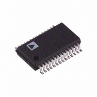
AD1871YRS Analog Devices Inc, AD1871YRS Datasheet - Page 16

AD1871YRS
Manufacturer Part Number
AD1871YRS
Description
IC ADC STEREO AUDIO 24BIT 28SSOP
Manufacturer
Analog Devices Inc
Datasheet
1.AD1871YRSZ.pdf
(28 pages)
Specifications of AD1871YRS
Rohs Status
RoHS non-compliant
Number Of Bits
24
Sampling Rate (per Second)
96k
Data Interface
Serial, SPI™
Number Of Converters
2
Voltage Supply Source
Analog and Digital
Operating Temperature
-40°C ~ 105°C
Mounting Type
Surface Mount
Package / Case
28-SSOP (0.200", 5.30mm Width)
Available stocks
Company
Part Number
Manufacturer
Quantity
Price
Company:
Part Number:
AD1871YRS
Manufacturer:
AD
Quantity:
5 510
Company:
Part Number:
AD1871YRS
Manufacturer:
PHILIPS
Quantity:
5 510
Company:
Part Number:
AD1871YRSZ
Manufacturer:
AD
Quantity:
114
Part Number:
AD1871YRSZ
Manufacturer:
ADI/亚德诺
Quantity:
20 000
AD1871
FUNCTIONAL DESCRIPTION
Clocking Scheme
The MCLK pin is the input for the master clock frequency to
the device. Nominally the MCLK frequency will be 256 ¥ f
correct operation of the device. However, if the user’s MCLK is
a multiple of 256 ¥ f
to divide down the MCLK frequency to a suitable internal master
clock frequency (IMCLK) using the MCLK divider block as
Modulator
The AD1871’s analog - modulator section comprises a
second order multibit implementation using Analog Device’s
proprietary technology for best performance. As shown in
Figure 9, the two analog integrator blocks are followed by a
Flash ADC section that generates the multibit samples. The
output of the Flash ADC, which is thermometer encoded, is decoded
to binary for output to the filter sections and is scrambled for
feedback to the two integrator stages.
The modulator is optimized for operation at a sampling rate
of 6.144 MHz (which is 128 ¥ f
64 ¥ f
(AMC Bit in Control Register I) is used to select the modulator
S
at 96 kHz sampling). The modulator clock control
ANALOG
INPUT
S
DIVIDER
(perhaps 512 ¥ f
DIVIDER
MCLK
IMCLK
12.288MHz/
24.576MHz
SECTION
ANALOG
6.144MHz
FROM
INPUT
MODULATOR
/1
MCLK
-
/2
/4
/2
S
at 48 kHz sampling and
MODCLK
Figure 8. Clocking Scheme to Modulator and Filter Engine
IMCLK
/3
S
6.144MHz
or 768 ¥ f
(CONT REG I)
FEEDBACK DACs
AMC BIT
0/1
S
Figure 9. Modulator Block Diagram
), it is possible
FILTER
SINC
S
384kHz/
768kHz
for
–16–
HALF-BAND
shown in Figure 8. The divide options can be chosen from pass-
through (/1), /2, or /3 corresponding with 256 ¥ f
768 ¥ f
trolled using the MCD1–MCD0 Bits of Control Register III.
(see Table XIII.)
The resulting internal MCLK (IMCLK) is used to run the
decimating and filtering engine and must be chosen to be at a
ratio of 256 ¥ f
FILTERS
clock (MODCLK) as a ratio from the IMCLK. The modulator
clock divider options are /2 (default) for 48 kHz operation and
/4 for 96 kHz operation. When operating with an IMCLK of
12.288 MHz, the default divider setting (/2) gives a modulator clock
of 6.144 MHz. When operating with an IMCLK of 24.576 MHz,
the alternate divider setting (/4) gives a modulator clock of
6.144 MHz (see Figure 8).
If it is required to operate the device at a different output sample
rate than those detailed above, perhaps 44.1 kHz or 88.2 kHz,
the decimation filter cutoff characteristics can then be determined
from the normalized frequency response plot shown in TPC 6.
FLASH
ADC
SCRAMBLER
S
MCLKs, respectively. The MCLK divider can be con-
48kHz/
96kHz
DECODER
THERMO-
S
BINARY
METER
.
TO
HIGH-PASS
FILTERS
DIGITAL
OUTPUT
(4 BITS/6.144MHz)
(CONT REG I)
HPE BIT
48kHz/
96kHz
S
, 512 ¥ f
REV. 0
S
, or


