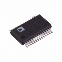
AD1871YRS Analog Devices Inc, AD1871YRS Datasheet - Page 25

AD1871YRS
Manufacturer Part Number
AD1871YRS
Description
IC ADC STEREO AUDIO 24BIT 28SSOP
Manufacturer
Analog Devices Inc
Datasheet
1.AD1871YRSZ.pdf
(28 pages)
Specifications of AD1871YRS
Rohs Status
RoHS non-compliant
Number Of Bits
24
Sampling Rate (per Second)
96k
Data Interface
Serial, SPI™
Number Of Converters
2
Voltage Supply Source
Analog and Digital
Operating Temperature
-40°C ~ 105°C
Mounting Type
Surface Mount
Package / Case
28-SSOP (0.200", 5.30mm Width)
Available stocks
Company
Part Number
Manufacturer
Quantity
Price
Company:
Part Number:
AD1871YRS
Manufacturer:
AD
Quantity:
5 510
Company:
Part Number:
AD1871YRS
Manufacturer:
PHILIPS
Quantity:
5 510
Company:
Part Number:
AD1871YRSZ
Manufacturer:
AD
Quantity:
114
Part Number:
AD1871YRSZ
Manufacturer:
ADI/亚德诺
Quantity:
20 000
INTERFACING
Analog Interfacing
The analog section of the AD1871 has been designed to offer
flexibility as well as high performance. Users may choose full
differential input directly to the ADC’s - modulator via Pins
CAPxP and CAPxN. Alternatively, when using the on-chip PGA
section, it is also possible to multiplex single-ended inputs on Pins
VINxP and VINxN or to use these pins for full differential input.
Whichever input topology is chosen (direct or via mux/PGA
section), the modulator input pins (CAPxP and CAPxN) require
capacitors to act as dynamic charge storage for the switched
capacitor input section. Component selection for these capacitors
is critical as the input audio signal appears on or across these
capacitors. A high quality dielectric is recommended for these
capacitors multilayer ceramic, NPO or metal film, PPS for
surface-mounted versions, and polypropylene for through-hole
versions. Indeed, as a general recommendation, high quality
dielectrics should be specified where capacitors are carrying the
input audio signal.
Modulator Direct Input
Figure 23 shows the connection of a single-ended source via an
external single-ended-to-differential converter to the modulator
input of the AD1871. The external amplifier/buffer should have
good slew rate characteristics to meet the dynamic characteristics
of the modulator input that is a switched-capacitor load.
The output of the external amplifier/buffer should be decoupled
from the input capacitors via a 250 W resistor (metal film).
In order to configure the AD1871 for differential input via the
CAPxP and CAPxN pins, the Mux/PGA section must be disabled
by setting the MEL and MER Bits in Control Register III to 1.
PGA Input, Single-Ended
Figure 24 shows the connection of a single-ended source to the
PGA section of the AD1871. The PGA section is configured
for single-ended-to-differential conversion. The differential
outputs are connected internally to the CAPxx pins via 250 W
series resistors.
In order to configure the AD1871 for single-ended input, the
Control Registers must be configured as follows:
REV. 0
FERRITE
Figure 23. Direct Connection to Modulator
100pF
NPO
10 F
5.76k
5.76k
750k
OP275
OP275
5.76k
120pF
5.76k
NPO
10 F
237
237
100nF
100pF
NPO
NPO
1nF
100pF
NPO
CAPLP
AD1871
CAPLN
VREF
–25–
Left Channel
Control Register I = xx0xGGGxxx, where GGG = the Input Gain
(see Table V).
Control Register III = 00xx1x0Sxx, where S = the SE Channel
Selection.
Right Channel
Control Register I = xx0xxxxGGG, where GGG = the Input Gain
(see Table V).
Control Register III = 00xxx1xx0S, where S = the SE Channel
Selection.
PGA Input, Differential
Figure 25 shows the connection of a differential source to the PGA
section of the AD1871. The PGA section is configured as a
differential buffer. The buffered differential outputs are con-
nected internally to the CAPxx pins via a 250 W series resistors.
In order to configure the AD1871 for differential input via the
Mux/PGA, the Control Registers must be configured as follows:
Left Channel
Control Register I = xx0xGGGxxx, where GGG = the Input Gain
(see Table V).
Control Register III = 00xx0x0xxx.
Right Channel
Control Register I = xx0xxxxGGG, where GGG = the Input Gain
(see Table V).
Control Register III = 00xxx0xx0x.
Figure 24. Single-Ended Input via PGA Section
Figure 25. Differential Input via PGA Section
FERRITE
2
3
1
600Z
100pF
100pF
NPO
NPO
100pF
10 F
NPO
10 F
10 F
10 F
10 F
100pF
NPO
NPO
100nF
1nF
100pF
NPO
NPO
100nF
1nF
AD1871
CAPLP
VINLP
VINLN
VREF
CAPLN
AD1871
CAPLP
VREF
CAPLN
VINLP
VINLN
AD1871


