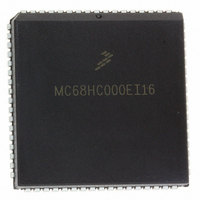
MC68HC000EI16 Freescale Semiconductor, MC68HC000EI16 Datasheet - Page 81

MC68HC000EI16
Manufacturer Part Number
MC68HC000EI16
Description
IC MPU 32BIT 16MHZ 68-PLCC
Manufacturer
Freescale Semiconductor
Specifications of MC68HC000EI16
Processor Type
M680x0 32-Bit
Speed
16MHz
Voltage
3.3V, 5V
Mounting Type
Surface Mount
Package / Case
68-PLCC
Family Name
M68000
Device Core
ColdFire
Device Core Size
16/32Bit
Frequency (max)
16MHz
Instruction Set Architecture
RISC
Supply Voltage 1 (typ)
5V
Operating Supply Voltage (max)
5.25V
Operating Supply Voltage (min)
4.75V
Operating Temp Range
0C to 70C
Operating Temperature Classification
Commercial
Mounting
Surface Mount
Pin Count
68
Package Type
PLCC
Lead Free Status / RoHS Status
Lead free / RoHS Compliant
Features
-
Lead Free Status / Rohs Status
Compliant
Available stocks
Company
Part Number
Manufacturer
Quantity
Price
Company:
Part Number:
MC68HC000EI16
Manufacturer:
TI
Quantity:
604
Company:
Part Number:
MC68HC000EI16
Manufacturer:
FREESCALE
Quantity:
2 900
Company:
Part Number:
MC68HC000EI16
Manufacturer:
Freescale Semiconductor
Quantity:
10 000
Company:
Part Number:
MC68HC000EI16R2
Manufacturer:
FREESCAL
Quantity:
8 831
Company:
Part Number:
MC68HC000EI16R2
Manufacturer:
Freescale Semiconductor
Quantity:
10 000
In the MC68010, the BERR signal can be delayed after the assertion of DTACK.
Specification #48 is the maximum time between assertion of DTACK and assertion of
BERR. If this maximum delay is exceeded, operation of the processor may be erratic.
5.8 SYNCHRONOUS OPERATION
In some systems, external devices use the system clock to generate DTACK and other
asynchronous input signals. This synchronous operation provides a closely coupled
design with maximum performance, appropriate for frequently accessed parts of the
system. For example, memory can operate in the synchronous mode, but peripheral
devices operate asynchronously. For a synchronous device, the designer uses explicit
timing information shown in Section 10 Electrical Characteristics. These specifications
define the state of all bus signals relative to a specific state of the processor clock.
The standard M68000 bus cycle consists of four clock periods (eight bus cycle states)
and, optionally, an integral number of clock cycles inserted as wait states. Wait states are
inserted as required to allow sufficient response time for the external device. The following
state-by-state description of the bus cycle differs from those descriptions in 5.1.1 READ
CYCLE and 5.1.2 WRITE CYCLE by including information about the important timing
parameters that apply in the bus cycle states.
STATE 0
MOTOROLA
UDS/LDS
DTACK
DATA
ADDR
R/W
AS
The bus cycle starts in S0, during which the clock is high. At the rising edge
of S0, the function code for the access is driven externally. Parameter #6A
defines the delay from this rising edge until the function codes are valid.
Also, the R/W signal is driven high; parameter #18 defines the delay from
the same rising edge to the transition of R/W . The minimum value for
parameter #18 applies to a read cycle preceded by a write cycle; this value
M68000 8-/16-/32-BIT MICROPROCESSORS USER'S MANUAL
Figure 5-34. Pseudo-Asynchronous Write Cycle
Freescale Semiconductor, Inc.
For More Information On This Product,
11
20A
55
Go to: www.freescale.com
22
26
28
29
5- 35


