TP3070V-XG National Semiconductor, TP3070V-XG Datasheet - Page 14
TP3070V-XG
Manufacturer Part Number
TP3070V-XG
Description
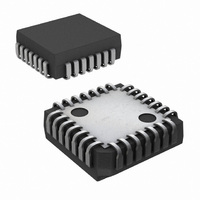
IC COMBO II PCM FILTER 28PLCC
Manufacturer
National Semiconductor
Series
COMBO®IIr
Type
PCM Codec/Filterr
Datasheet
1.TP3070V-GNOPB.pdf
(26 pages)
Specifications of TP3070V-XG
Data Interface
PCM Audio Interface
Number Of Adcs / Dacs
1 / 1
Sigma Delta
No
Voltage - Supply, Analog
±5V
Voltage - Supply, Digital
±5V
Operating Temperature
-40°C ~ 85°C
Mounting Type
Surface Mount
Package / Case
28-LCC (J-Lead)
Lead Free Status / RoHS Status
Contains lead / RoHS non-compliant
Other names
*TP3070V-XG
Available stocks
Company
Part Number
Manufacturer
Quantity
Price
Company:

Part Number:
TP3070V-XG
Manufacturer:
NSC
Quantity:
5 510
Company:
Part Number:
TP3070V-XG
Manufacturer:
Texas Instruments
Quantity:
10 000
Part Number:
TP3070V-XG
Manufacturer:
NS/国半
Quantity:
20 000
Company:
Part Number:
TP3070V-XG/NOPB
Manufacturer:
Texas Instruments
Quantity:
10 000


www.national.com
SERIAL CONTROL PORT TIMING
t
t
INTERFACE LATCH TIMING
t
t
t
MASTER RESET PIN
t
Symbol
DSD
DDZ
SLC
HCL
DCL
WMR
Unless otherwise noted, limits printed in BOLD characters are guaranteed for V
+70˚C (−40˚C to +85˚C for TP3070-X) by correlation with 100% electrical testing at T
correlation with other production tests and/or product design and characterization. All signals referenced to GND. Typicals
specified at V
All timing parameters are measured at V
See Definitions and Timing Conventions section for test methods information.
Timing Specifications
Note 11: Applies only to MCLK Frequencies
Timing Diagrams
Delay Time, CS Low
to CO (CI/O) Valid
Delay Time, CS or 9th CCLK
High to CO (CI/O) High
Impedance
Setup Time, IL to
CCLK 8 of Byte 1
Hold Time, IL Valid from
8th CCLK Low (Byte 1)
Delay Time CCLK 8 of
Byte 2 to IL
Duration of
Master Reset High
CC
= +5V, V
Parameter
BB
= −5V, T
1.536 MHz. At 512 kHz a 50:50
(Continued)
A
= 25˚C.
OH
FIGURE 4. Non Delayed Data Timing Mode
= 2.0V and V
Applies Only if Separate
CS used for Byte 2
−40˚C to +85˚C (TP3070-X)
Applies to Earlier of CS High or 9th
CCLK High
Interface Latch Inputs Only
Interface Latch Outputs Only
C
L
= 50 pF
OL
Conditions
= 0.7V.
14
±
2% Duty Cycle must be used.
CC
= +5V
A
= 25˚C. All other limits are assured by
Min
100
15
50
1
±
5%; V
Typ
BB
= −5V
Max
100
200
±
80
80
5%; T
A
DS008635-8
= 0˚C to
Units
ns
ns
ns
ns
ns
ns
µs
Related parts for TP3070V-XG
Image
Part Number
Description
Manufacturer
Datasheet
Request
R

Part Number:
Description:
IC INTERFAC PCM COMBO II 28-PLCC
Manufacturer:
National Semiconductor
Datasheet:

Part Number:
Description:
IC COMBO II EXT.TEMP. 28PLCC
Manufacturer:
National Semiconductor
Datasheet:

Part Number:
Description:
Audio CODEC IC
Manufacturer:
National Semiconductor
Datasheet:

Part Number:
Description:
Manufacturer:
National Semiconductor
Datasheet:
Part Number:
Description:
IC,PCM CODEC,SINGLE,CMOS,LDCC,28PIN,PLASTIC
Manufacturer:
National Semiconductor

Part Number:
Description:
Combo Ii Programmable Pcm Codec/filter
Manufacturer:
National Semiconductor Corporation
Datasheet:

Part Number:
Description:
TRISILTM
Manufacturer:
STMicroelectronics
Datasheet:
Part Number:
Description:
National Semiconductor [8-Bit D/A Converter]
Manufacturer:
National Semiconductor
Datasheet:
Part Number:
Description:
National Semiconductor [Media Coprocessor]
Manufacturer:
National Semiconductor
Datasheet:
Part Number:
Description:
Digitally Controlled Tone and Volume Circuit with Stereo Audio Power Amplifier, Microphone Preamp Stage and National 3D Sound
Manufacturer:
National Semiconductor
Datasheet: