TP3070V-XG National Semiconductor, TP3070V-XG Datasheet - Page 9
TP3070V-XG
Manufacturer Part Number
TP3070V-XG
Description
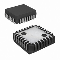
IC COMBO II PCM FILTER 28PLCC
Manufacturer
National Semiconductor
Series
COMBO®IIr
Type
PCM Codec/Filterr
Datasheet
1.TP3070V-GNOPB.pdf
(26 pages)
Specifications of TP3070V-XG
Data Interface
PCM Audio Interface
Number Of Adcs / Dacs
1 / 1
Sigma Delta
No
Voltage - Supply, Analog
±5V
Voltage - Supply, Digital
±5V
Operating Temperature
-40°C ~ 85°C
Mounting Type
Surface Mount
Package / Case
28-LCC (J-Lead)
Lead Free Status / RoHS Status
Contains lead / RoHS non-compliant
Other names
*TP3070V-XG
Available stocks
Company
Part Number
Manufacturer
Quantity
Price
Company:

Part Number:
TP3070V-XG
Manufacturer:
NSC
Quantity:
5 510
Company:
Part Number:
TP3070V-XG
Manufacturer:
Texas Instruments
Quantity:
10 000
Part Number:
TP3070V-XG
Manufacturer:
NS/国半
Quantity:
20 000
Company:
Part Number:
TP3070V-XG/NOPB
Manufacturer:
Texas Instruments
Quantity:
10 000


Programmable Functions
Three registers must be programmed in COMBO II to fully
configure the Hybrid Balance Filter as follows:
Register 1: select/de-select Hybrid Balance Filter;
Register 2: select/de-select Hybal1 filter;
Register 3: program pole frequency in Hybal2 filter;
Standard filter design techniques may be used to model the
echo path (see Equation (1) ) and design a matching hybrid
balance filter configuration. Alternatively, the frequency re-
sponse of the echo path can be measured and the hybrid
balance filter designed to replicate it.
A Hybrid Balance filter design guide and software optimiza-
tion program are available under license from National Semi-
conductor Corporation; order TP3077SW.
Applications Information
Figure 3 shows a typical application of the TP3071 together
with a typical monolithic SLIC. Four of the IL latches are con-
figured as outputs to control the relay drivers on the SLIC,
while IL4 is an input for the Supervision signal.
invert/non-invert cancellation signal;
select/de-select Hybal2 filter section;
attenuator setting.
set Hybal1 to 2nd order or 1st order;
pole and zero frequency selection.
program zero frequency in Hybal2 filter.
FIGURE 2. Simplified Diagram of Hybrid Balance Circuit
(Continued)
9
POWER SUPPLIES
While the pins of the TP3070 COMBO II devices are well
protected against electrical misuse, it is recommended that
the standard CMOS practice of applying GND to the device
before any other connections are made should always be
followed. In applications where the printed circuit card may
be plugged into a hot socket with power and clocks already
present, extra long pins on the connector should be used for
ground and V
nected between V
To minimize noise sources, all ground connections to each
device should meet at a common point as close as possible
to the device GND pin in order to prevent the interaction of
ground return currents flowing through a common bus im-
pedance. Power supply decoupling capacitors of 0.1 µF
should be connected from this common device ground point
to V
and V
Resistance Capacitors of at least 10 µF located near the
card edge connector.
Further guidelines on PCB layout techniques are provided in
Application Note AN-614, “ COMBO II
CODEC/Filter Family Application Guide”.
CC
BB
and V
should also be decoupled with Low Effective Series
BB
BB
. In addition, a Schottky diode should be con-
as close to the device pins as possible. V
BB
and ground.
DS008635-5
™
Programmable PCM
www.national.com
CC
Related parts for TP3070V-XG
Image
Part Number
Description
Manufacturer
Datasheet
Request
R

Part Number:
Description:
IC INTERFAC PCM COMBO II 28-PLCC
Manufacturer:
National Semiconductor
Datasheet:

Part Number:
Description:
IC COMBO II EXT.TEMP. 28PLCC
Manufacturer:
National Semiconductor
Datasheet:

Part Number:
Description:
Audio CODEC IC
Manufacturer:
National Semiconductor
Datasheet:

Part Number:
Description:
Manufacturer:
National Semiconductor
Datasheet:
Part Number:
Description:
IC,PCM CODEC,SINGLE,CMOS,LDCC,28PIN,PLASTIC
Manufacturer:
National Semiconductor

Part Number:
Description:
Combo Ii Programmable Pcm Codec/filter
Manufacturer:
National Semiconductor Corporation
Datasheet:

Part Number:
Description:
TRISILTM
Manufacturer:
STMicroelectronics
Datasheet:
Part Number:
Description:
National Semiconductor [8-Bit D/A Converter]
Manufacturer:
National Semiconductor
Datasheet:
Part Number:
Description:
National Semiconductor [Media Coprocessor]
Manufacturer:
National Semiconductor
Datasheet:
Part Number:
Description:
Digitally Controlled Tone and Volume Circuit with Stereo Audio Power Amplifier, Microphone Preamp Stage and National 3D Sound
Manufacturer:
National Semiconductor
Datasheet: