TP3070V-XG National Semiconductor, TP3070V-XG Datasheet - Page 6
TP3070V-XG
Manufacturer Part Number
TP3070V-XG
Description
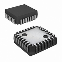
IC COMBO II PCM FILTER 28PLCC
Manufacturer
National Semiconductor
Series
COMBO®IIr
Type
PCM Codec/Filterr
Datasheet
1.TP3070V-GNOPB.pdf
(26 pages)
Specifications of TP3070V-XG
Data Interface
PCM Audio Interface
Number Of Adcs / Dacs
1 / 1
Sigma Delta
No
Voltage - Supply, Analog
±5V
Voltage - Supply, Digital
±5V
Operating Temperature
-40°C ~ 85°C
Mounting Type
Surface Mount
Package / Case
28-LCC (J-Lead)
Lead Free Status / RoHS Status
Contains lead / RoHS non-compliant
Other names
*TP3070V-XG
Available stocks
Company
Part Number
Manufacturer
Quantity
Price
Company:

Part Number:
TP3070V-XG
Manufacturer:
NSC
Quantity:
5 510
Company:
Part Number:
TP3070V-XG
Manufacturer:
Texas Instruments
Quantity:
10 000
Part Number:
TP3070V-XG
Manufacturer:
NS/国半
Quantity:
20 000
Company:
Part Number:
TP3070V-XG/NOPB
Manufacturer:
Texas Instruments
Quantity:
10 000


www.national.com
Programmable Functions
vice is powered-up or down by setting the “P” bit as indi-
cated. When the power-up or down control is entered as a
single byte instruction, bit one (1) must be reset to a 0.
When a power-up command is given, all de-activated circuits
are activated, but the TRI-STATE PCM output(s), D
D
ond FS
2.0 CONTROL REGISTER INSTRUCTION
The first byte of a READ or WRITE instruction to the Control
Register is as shown in Table 1 . The second byte has the fol-
lowing bit functions:
Note 4: State at power-on initialization. (Bit 4 = 0)
2.1 Master Clock Frequency Selection
A Master clock must be provided to COMBO II for operation
of the filter and coding/decoding functions. The MCLK fre-
quency must be either 512 kHz, 1.536 MHz, 1.544 MHz,
2.048 MHz, or 4.096 MHz and must be synchronous with
BCLK. Bits F
ization to select the correct internal divider.
2.2 Coding Law Selection
Bits “MA” and “IA” in Table 2 permit the selection of µ255
coding or A-law coding, with or without even bit inversion.
2.3 Analog Loopback
Analog Loopback mode is entered by setting the “AL” and
“DL” bits in the Control Register as shown in Table 2 . In the
analog loopback mode, the Transmit input VF
from the input pin and internally connected to the VF
put, forming a loop from the Receive PCM Register back to
the Transmit PCM Register. The VF
and the programmed settings of the Transmit and Receive
F
X
7
0
0
1
1
1
1), will remain in the high impedance state until the sec-
F
6
0
1
0
1
TABLE 2. Control Register Byte 2 Functions
0
X
Bit Number and Name
pulse after power-up.
MA
5
0
1
1
1
and F
IA
4
X
0
1
DN
3
0
1
0
(see Table 2 ) must be set during initial-
DL
2
0
1
0
AL
X
1
0
1
PP
0
0
1
MCLK = 512 kHz
MCLK = 1.536
or 1.544 MHz
MCLK = 2.048 MHz
(Note 4)
MCLK = 4.096 MHz
Select µ-255 law (Note 4)
A-law, Including Even
Bit Inversion
A-law, No Even Bit Inversion
Delayed Data Timing
Non-Delayed Data
Timing (Note 4)
Normal Operation
(Note 4)
Digital Loopback
Analog Loopback
Power Amp Enabled in PDN
Power Amp Disabled in
PDN (Note 4)
R
O pin remains active,
Function
(Continued)
X
I is isolated
X
R
0 (and
O out-
6
gains remain unchanged, thus care must be taken to ensure
that overload levels are not exceeded anywhere in the loop.
Hybrid balance must be disabled for meaningful analog loop-
back function.
2.4 Digital Loopback
Digital Loopback mode is entered by setting the “AL” and
“DL” bits in the Control Register as shown in Table 2 . This
mode provides another stage of path verification by enabling
data written into the Receive PCM Register to be read back
from that register in any Transmit time-slot at D
loopback, the decoder will remain functional and output a
signal at VF
be turned off by programming the receive gain register to all
zeros.
3.0 INTERFACE LATCH DIRECTIONS
Immediately following power-on, all Interface Latches as-
sume they are inputs, and therefore all IL pins are in a high
impedance state. Each IL pin may be individually pro-
grammed as a logic input or output by writing the appropriate
instruction to the LDR, see Table 1 and Table 3 . For mini-
mum power dissipation, unconnected latch pins should be
programmed as outputs. For the TP3071, L5 should always
be programmed as an output.
Bits L
the LDR with the L bits in the second byte set as follows:
X = don’t care
INTERFACE LATCH STATES
Interface Latches configured as outputs assume the state
determined by the appropriate data bit in the 2-byte instruc-
tion written to the Interface Latch Register (ILR) as shown in
Table 1 and Table 4 . Latches configured as inputs will sense
the state applied by an external source, such as the
Off-Hook detect output of a SLIC. All bits of the ILR, i.e.
sensed inputs and the programmed state of outputs, can be
read back in the 2nd byte of a READ from the ILR.
It is recommended that during initialization, the state of IL
pins to be configured as outputs should be programmed first,
followed immediately by the Latch Direction Register.
TABLE 3. Byte 2 Functions of Latch Direction Register
D
L
7
7
0
0
5
–L
TABLE 4. Interface Latch Data Bit Order
0
L
D
L
6
6
must be set by writing the specified instruction to
n
1
1
R
0
1
Bit
O. If this is undesirable, the receive output can
D
L
5
5
2
2
Byte 2 Bit Number
Bit Number
D
L
4
4
3
3
D
L
3
3
4
4
IL Direction
Output
Input
D
L
2
2
5
5
X
0/1. In digital
X
X
1
1
0
X
0
X
Related parts for TP3070V-XG
Image
Part Number
Description
Manufacturer
Datasheet
Request
R

Part Number:
Description:
IC INTERFAC PCM COMBO II 28-PLCC
Manufacturer:
National Semiconductor
Datasheet:

Part Number:
Description:
IC COMBO II EXT.TEMP. 28PLCC
Manufacturer:
National Semiconductor
Datasheet:

Part Number:
Description:
Audio CODEC IC
Manufacturer:
National Semiconductor
Datasheet:

Part Number:
Description:
Manufacturer:
National Semiconductor
Datasheet:
Part Number:
Description:
IC,PCM CODEC,SINGLE,CMOS,LDCC,28PIN,PLASTIC
Manufacturer:
National Semiconductor

Part Number:
Description:
Combo Ii Programmable Pcm Codec/filter
Manufacturer:
National Semiconductor Corporation
Datasheet:

Part Number:
Description:
TRISILTM
Manufacturer:
STMicroelectronics
Datasheet:
Part Number:
Description:
National Semiconductor [8-Bit D/A Converter]
Manufacturer:
National Semiconductor
Datasheet:
Part Number:
Description:
National Semiconductor [Media Coprocessor]
Manufacturer:
National Semiconductor
Datasheet:
Part Number:
Description:
Digitally Controlled Tone and Volume Circuit with Stereo Audio Power Amplifier, Microphone Preamp Stage and National 3D Sound
Manufacturer:
National Semiconductor
Datasheet: