TP3070V-XG National Semiconductor, TP3070V-XG Datasheet - Page 21
TP3070V-XG
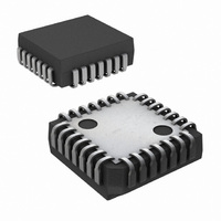
Manufacturer Part Number
TP3070V-XG
Description
IC COMBO II PCM FILTER 28PLCC
Manufacturer
National Semiconductor
Series
COMBO®IIr
Type
PCM Codec/Filterr
Datasheet
1.TP3070V-GNOPB.pdf
(26 pages)
Specifications of TP3070V-XG
Data Interface
PCM Audio Interface
Number Of Adcs / Dacs
1 / 1
Sigma Delta
No
Voltage - Supply, Analog
±5V
Voltage - Supply, Digital
±5V
Operating Temperature
-40°C ~ 85°C
Mounting Type
Surface Mount
Package / Case
28-LCC (J-Lead)
Lead Free Status / RoHS Status
Contains lead / RoHS non-compliant
Other names
*TP3070V-XG
Available stocks
Company
Part Number
Manufacturer
Quantity
Price
Company:

Part Number:
TP3070V-XG
Manufacturer:
NSC
Quantity:
5 510
Company:
Part Number:
TP3070V-XG
Manufacturer:
Texas Instruments
Quantity:
10 000
Part Number:
TP3070V-XG
Manufacturer:
NS/国半
Quantity:
20 000
Company:
Part Number:
TP3070V-XG/NOPB
Manufacturer:
Texas Instruments
Quantity:
10 000


Symbol
CROSSTALK
CT
CT
Transmission Characteristics
+70˚C (−40˚C to +85˚C for TP3070-X) by correlation with 100% electrical testing at T
0 dBm0, D
Note 12: Measured by grounded input at VF
Note 13: PPSR
Note 14: A signal is Valid if it is above V
Note 15: A multi-tone test technique is used.
Unless otherwise noted, limits printed in BOLD characters are guaranteed for V
gain), hybrid balance filter disabled. All other limits are assured by correlation with other production tests and/or product de-
sign and characterization. All signals referenced to GND. Typicals specified at V
X-R
R-X
a) All input signals are defined as: V
b) t
c) Delay Times are measured from the input signal Valid to the output signal Valid.
d) Setup Times are measured from the data input Valid to the clock input Invalid.
e) Hold Times are measured from the clock signal Valid to the data input Invalid.
f) Pulse widths are measured from V
R
is measured from V
Transmit to Receive
Crosstalk, 0 dBm0 Transmit
Level
Receive to Transmit
Crosstalk, 0 dBm0 Receive
Level
R
0 or D
X
, NPSR
R
Parameter
1 = 0 dBm0 PCM code. Transmit and receive gains programmed for maximum 0 dBm0 test levels (0 dB
X
, and CT
IL
to V
IH
R–X
. t
F
IL
IL
are measured with a −50 dBm0 activation signal applied to VF
is measured from V
IH
= 0.4V, V
to V
or below V
X
IL
I.
or from V
IH
IL
= 2.7V, t
f = 300 Hz–3400 Hz
D
f = 300 Hz–3400 Hz
(Note 13)
and Invalid if it is between V
R
IH
= Idle Code
IH
to V
R
to V
<
IH
(Continued)
.
IL
10 ns, t
.
F
<
Conditions
10 ns.
21
IL
and V
IH
. For the purposes of this specification the following conditions apply:
CC
X
CC
I.
= +5V
= +5V, V
A
= 25˚C. f = 1015.625 Hz, VF
±
5%, V
BB
Min
= −5V, T
BB
= −5V
Typ
−90
−90
A
= 25˚C.
±
5%; T
Max
−75
−70
www.national.com
A
X
I =
= 0˚C to
Units
dB
dB
Related parts for TP3070V-XG
Image
Part Number
Description
Manufacturer
Datasheet
Request
R

Part Number:
Description:
IC INTERFAC PCM COMBO II 28-PLCC
Manufacturer:
National Semiconductor
Datasheet:

Part Number:
Description:
IC COMBO II EXT.TEMP. 28PLCC
Manufacturer:
National Semiconductor
Datasheet:

Part Number:
Description:
Audio CODEC IC
Manufacturer:
National Semiconductor
Datasheet:

Part Number:
Description:
Manufacturer:
National Semiconductor
Datasheet:
Part Number:
Description:
IC,PCM CODEC,SINGLE,CMOS,LDCC,28PIN,PLASTIC
Manufacturer:
National Semiconductor

Part Number:
Description:
Combo Ii Programmable Pcm Codec/filter
Manufacturer:
National Semiconductor Corporation
Datasheet:

Part Number:
Description:
TRISILTM
Manufacturer:
STMicroelectronics
Datasheet:
Part Number:
Description:
National Semiconductor [8-Bit D/A Converter]
Manufacturer:
National Semiconductor
Datasheet:
Part Number:
Description:
National Semiconductor [Media Coprocessor]
Manufacturer:
National Semiconductor
Datasheet:
Part Number:
Description:
Digitally Controlled Tone and Volume Circuit with Stereo Audio Power Amplifier, Microphone Preamp Stage and National 3D Sound
Manufacturer:
National Semiconductor
Datasheet: