TP3070V-XG National Semiconductor, TP3070V-XG Datasheet - Page 4
TP3070V-XG
Manufacturer Part Number
TP3070V-XG
Description
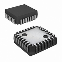
IC COMBO II PCM FILTER 28PLCC
Manufacturer
National Semiconductor
Series
COMBO®IIr
Type
PCM Codec/Filterr
Datasheet
1.TP3070V-GNOPB.pdf
(26 pages)
Specifications of TP3070V-XG
Data Interface
PCM Audio Interface
Number Of Adcs / Dacs
1 / 1
Sigma Delta
No
Voltage - Supply, Analog
±5V
Voltage - Supply, Digital
±5V
Operating Temperature
-40°C ~ 85°C
Mounting Type
Surface Mount
Package / Case
28-LCC (J-Lead)
Lead Free Status / RoHS Status
Contains lead / RoHS non-compliant
Other names
*TP3070V-XG
Available stocks
Company
Part Number
Manufacturer
Quantity
Price
Company:

Part Number:
TP3070V-XG
Manufacturer:
NSC
Quantity:
5 510
Company:
Part Number:
TP3070V-XG
Manufacturer:
Texas Instruments
Quantity:
10 000
Part Number:
TP3070V-XG
Manufacturer:
NS/国半
Quantity:
20 000
Company:
Part Number:
TP3070V-XG/NOPB
Manufacturer:
Texas Instruments
Quantity:
10 000


www.national.com
Functional Description
POWER-DOWN STATE
Following a period of activity in the powered-up state the
power-down state may be re-entered by writing any of the
control instructions into the serial control port with the “P” bit
set to “1” as indicated in Table 1 . It is recommended that the
chip be powered down before writing any additional instruc-
tions. In the power-down state, all non-essential circuitry is
de-activated and the D
impedance TRI-STATE condition.
The coefficients stored in the Hybrid Balance circuit and the
Gain Control registers, the data in the LDR and ILR, and all
control bits remain unchanged in the power-down state un-
less changed by writing new data via the serial control port,
which remains active. The outputs of the Interface Latches
also remain active, maintaining the ability to monitor and
control the SLIC.
TRANSMIT FILTER AND ENCODER
The Transmit section input, VF
ming input which is used as the differencing point for the in-
ternal hybrid balance cancellation signal. No external com-
ponents are necessary to set the gain. Following this circuit
is a programmable gain/attenuation amplifier which is con-
trolled by the contents of the Transmit Gain Register (see
Programmable Functions section). An active pre-filter then
precedes the 3rd order high-pass and 5th order low-pass
switched capacitor filters. The A/D converter has a com-
pressing characteristic according to the standard CCITT A or
µ255 coding laws, which must be selected by a control in-
struction during initialization (see Table 1 and Table 2 ). A pre-
cision on-chip voltage reference ensures accurate and highly
stable transmission levels. Any offset voltage arising in the
gain-set amplifier, the filters or the comparator is canceled by
an internal auto-zero circuit.
Each encode cycle begins immediately following the as-
signed Transmit time-slot. The total signal delay referenced
to the start of the time-slot is approximately 165 µs (due to
the Transmit Filter) plus 125 µs (due to encoding delay),
which totals 290 µs. Data is shifted out on D
the selected time slot on eight rising edges of BCLK.
DECODER AND RECEIVE FILTER
PCM data is shifted into the Decoder’s Receive PCM Regis-
ter via the D
the 8 falling edges of BCLK. The Decoder consists of an ex-
panding DAC with either A or µ255 law decoding character-
istic, which is selected by the same control instruction used
to select the Encode law during initialization. Following the
Decoder is a 5th order low-pass switched capacitor filter with
integral Sin x/x correction for the 8 kHz sample and hold. A
programmable gain amplifier, which must be set by writing to
the Receive Gain Register, is included, and finally a Power
Amplifier capable of driving a 300
load to
±
3.8V or a 15 k
R
0 or D
R
1 pin during the selected time-slot on
X
0 (and D
load to
X
I, is a high impedance sum-
X
±
1) outputs are in the high
4.0V at peak overload.
load to
(Continued)
X
0 or D
±
3.5V, a 600
X
1 during
4
A decode cycle begins immediately after the assigned re-
ceive time-slot, and 10 µs later the Decoder DAC output is
updated. The total signal delay is 10 µs plus 120 µs (filter de-
lay) plus 62.5 µs (
µs.
PCM INTERFACE
The FS
ning of the 8-bit transmit and receive time-slots respectively.
They may have any duration from a single cycle of BCLK
HIGH to one MCLK period LOW. Two different relationships
may be established between the frame sync inputs and the
actual time-slots on the PCM busses by setting bit 3 in the
Control Register (see Table 2 ). Non-delayed data mode is
similar to long-frame timing on the TP3050/60 series of de-
vices (COMBO); time-slots begin nominally coincident with
the rising edge of the appropriate FS input. The alternative is
to use Delayed Data mode, which is similar to short-frame
sync timing on COMBO, in which each FS input must be high
at least a half-cycle of BCLK earlier than the time-slot. The
Time-Slot Assignment circuit on the device can only be used
with Delayed Data timing.
When using Time-Slot Assignment, the beginning of the first
time-slot in a frame is identified by the appropriate FS input.
The actual transmit and receive time-slots are then deter-
mined by the internal Time-Slot Assignment counters.
Transmit and Receive frames and time-slots may be skewed
from each other by any number of BCLK cycles. During each
assigned Transmit time-slot, the selected D
data out from the PCM register on the rising edges of BCLK.
TS
bit times of the time-slot to control the TRI-STATE Enable of
a backplane line-driver. Serial PCM data is shifted into the
selected D
on the falling edges of BCLK. D
are selectable on the TP3070 only, see Section 6.
X
0 (or TS
X
and FS
R
0/1 input during each assigned Receive time-slot
X
1 as appropriate) also pulls low for the first 7
R
1
⁄
frame sync inputs determine the begin-
2
frame) which gives approximately 190
X
0 or D
X
1 and D
X
0/1 output shifts
R
0 or D
R
1
⁄
1
2
Related parts for TP3070V-XG
Image
Part Number
Description
Manufacturer
Datasheet
Request
R

Part Number:
Description:
IC INTERFAC PCM COMBO II 28-PLCC
Manufacturer:
National Semiconductor
Datasheet:

Part Number:
Description:
IC COMBO II EXT.TEMP. 28PLCC
Manufacturer:
National Semiconductor
Datasheet:

Part Number:
Description:
Audio CODEC IC
Manufacturer:
National Semiconductor
Datasheet:

Part Number:
Description:
Manufacturer:
National Semiconductor
Datasheet:
Part Number:
Description:
IC,PCM CODEC,SINGLE,CMOS,LDCC,28PIN,PLASTIC
Manufacturer:
National Semiconductor

Part Number:
Description:
Combo Ii Programmable Pcm Codec/filter
Manufacturer:
National Semiconductor Corporation
Datasheet:

Part Number:
Description:
TRISILTM
Manufacturer:
STMicroelectronics
Datasheet:
Part Number:
Description:
National Semiconductor [8-Bit D/A Converter]
Manufacturer:
National Semiconductor
Datasheet:
Part Number:
Description:
National Semiconductor [Media Coprocessor]
Manufacturer:
National Semiconductor
Datasheet:
Part Number:
Description:
Digitally Controlled Tone and Volume Circuit with Stereo Audio Power Amplifier, Microphone Preamp Stage and National 3D Sound
Manufacturer:
National Semiconductor
Datasheet: