TP3070V-XG National Semiconductor, TP3070V-XG Datasheet - Page 3
TP3070V-XG
Manufacturer Part Number
TP3070V-XG
Description
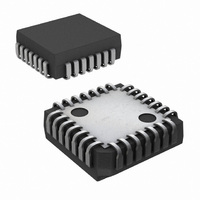
IC COMBO II PCM FILTER 28PLCC
Manufacturer
National Semiconductor
Series
COMBO®IIr
Type
PCM Codec/Filterr
Datasheet
1.TP3070V-GNOPB.pdf
(26 pages)
Specifications of TP3070V-XG
Data Interface
PCM Audio Interface
Number Of Adcs / Dacs
1 / 1
Sigma Delta
No
Voltage - Supply, Analog
±5V
Voltage - Supply, Digital
±5V
Operating Temperature
-40°C ~ 85°C
Mounting Type
Surface Mount
Package / Case
28-LCC (J-Lead)
Lead Free Status / RoHS Status
Contains lead / RoHS non-compliant
Other names
*TP3070V-XG
Available stocks
Company
Part Number
Manufacturer
Quantity
Price
Company:

Part Number:
TP3070V-XG
Manufacturer:
NSC
Quantity:
5 510
Company:
Part Number:
TP3070V-XG
Manufacturer:
Texas Instruments
Quantity:
10 000
Part Number:
TP3070V-XG
Manufacturer:
NS/国半
Quantity:
20 000
Company:
Part Number:
TP3070V-XG/NOPB
Manufacturer:
Texas Instruments
Quantity:
10 000


Pin Descriptions
FS
BCLK
MCLK
VF
VF
D
D
TS
TS
D
D
CCLK
X
X
R
R
Pin
R
X
R
0
1
X
X
0
1
I
0
1
O
Receive Frame Sync input. Normally a pulse
or squarewave with an 8 kHz repetition rate is
applied to this input to define the start of the
receive time slot assigned to this device
(non-delayed data timing mode), or the start of
the receive frame (delayed data timing mode
using the internal time-slot assignment
counter).
Bit clock input used to shift PCM data into and
out of the D
from 64 kHz to 4.096 MHz in 8 kHz
increments, and must be synchronous with
MCLK.
Master clock input used by the switched
capacitor filters and the encoder and decoder
sequencing logic. Must be 512 kHz, 1.536
MHz, 1.544 MHz, 2.048 MHz or 4.096 MHz
and synchronous with BCLK.
The Transmit analog high-impedance input.
Voice frequency signals present on this input
are encoded as an A-law or µ-law PCM bit
stream and shifted out on the selected D
The Receive analog power amplifier output,
capable of driving load impedances as low as
300
required). PCM data received on the assigned
D
as voice frequency signals.
D
available on all devices. These Transmit Data
TRI-STATE
impedance state except during the assigned
transmit time slot on the assigned port, during
which the transmit PCM data byte is shifted
out on the rising edges of BCLK.
TS
available on all devices. Normally these
open-drain outputs are floating in a high
impedance state except when a time-slot is
active on one of the D
appropriate TS
backplane line-driver.
D
available on all devices. These receive data
inputs are inactive except during the assigned
receive time slot of the assigned port when
the receive PCM data is shifted in on the
falling edges of BCLK.
Control Clock input. This clock shifts serial
control information into or out from CI/O or CI
and CO when the CS input is low, depending
on the current instruction. CCLK may be
asynchronous with the other system clocks.
R
X
R
1 is available on the TP3070 only; D
X
1 is available on the TP3070 only; D
pin is decoded and appears at this output
1 is available on the TP3070 only; TS
(depending on the peak overload level
®
R
outputs remain in the high
and D
X
output pulls low to enable a
Description
(Continued)
X
pins. BCLK may vary
X
outputs, when the
X
R
0 is
0 is
X
X
pin.
0 is
3
Functional Description
POWER-ON INITIALIZATION
When power is first applied, power-on reset circuitry initial-
izes the COMBO II and puts it into the power-down state.
The gain control registers for the transmit and receive gain
sections are programmed to OFF (00000000), the hybrid
balance circuit is turned off, the power amp is disabled and
the device is in the non-delayed timing mode. The Latch Di-
rection Register (LDR) is pre-set with all IL pins programmed
as inputs, placing the SLIC interface pins in a high imped-
ance state. The CI/O pin is set as an input ready for the first
control byte of the initialization sequence. Other initial states
in the Control Register are indicated in Section 2.0.
A reset to these same initial conditions may also be forced by
driving the MR pin momentarily high. This may be done ei-
ther when powered-up or down. For normal operation this
pin must be pulled low. If not used, MR should be hard-wired
to ground.
The desired modes for all programmable functions may be
initialized via the control port prior to a Power-up command.
CI/O
CI
CO
CS
IL5–IL0
MR
NC
Pin
This is the Control Data I/O pin which is
provided on the TP3071. Serial control
information is shifted to or read from COMBO
II on this pin when CS is low. The direction of
the data is determined by the current
instruction as defined in Table 1 .
This is a separate Control Input, available only
on the TP3070. It can be connected to CO if
required.
This is a separate Control Output, available
only on the TP3070. It can be connected to CI
if required.
Chip Select input. When this pin is low, control
information can be written to or read from
COMBO II via the CI/O pin (or CI and CO).
IL5 through IL0 are available on the TP3070.
IL4 through IL0 are available on the TP3071.
Each Interface Latch I/O pin may be
individually programmed as an input or an
output determined by the state of the
corresponding bit in the Latch Direction
Register (LDR). For pins configured as inputs,
the logic state sensed on each input is latched
into the Interface Latch Register (ILR)
whenever control data is written to COMBO II,
while CS is low, and the information is shifted
out on the CO (or CI/O) pin. When configured
as outputs, control data written into the ILR
appears at the corresponding IL pins.
This logic input must be pulled low for normal
operation of COMBO II. When pulled
momentarily high (at least 1 µsec.), all
programmable registers in the device are reset
to the states specified under “Power-On
Initialization”.
No Connection. Do not connect to this pin. Do
not route traces through this pin.
Description
www.national.com
Related parts for TP3070V-XG
Image
Part Number
Description
Manufacturer
Datasheet
Request
R

Part Number:
Description:
IC INTERFAC PCM COMBO II 28-PLCC
Manufacturer:
National Semiconductor
Datasheet:

Part Number:
Description:
IC COMBO II EXT.TEMP. 28PLCC
Manufacturer:
National Semiconductor
Datasheet:

Part Number:
Description:
Audio CODEC IC
Manufacturer:
National Semiconductor
Datasheet:

Part Number:
Description:
Manufacturer:
National Semiconductor
Datasheet:
Part Number:
Description:
IC,PCM CODEC,SINGLE,CMOS,LDCC,28PIN,PLASTIC
Manufacturer:
National Semiconductor

Part Number:
Description:
Combo Ii Programmable Pcm Codec/filter
Manufacturer:
National Semiconductor Corporation
Datasheet:

Part Number:
Description:
TRISILTM
Manufacturer:
STMicroelectronics
Datasheet:
Part Number:
Description:
National Semiconductor [8-Bit D/A Converter]
Manufacturer:
National Semiconductor
Datasheet:
Part Number:
Description:
National Semiconductor [Media Coprocessor]
Manufacturer:
National Semiconductor
Datasheet:
Part Number:
Description:
Digitally Controlled Tone and Volume Circuit with Stereo Audio Power Amplifier, Microphone Preamp Stage and National 3D Sound
Manufacturer:
National Semiconductor
Datasheet: