TP3070V-XG National Semiconductor, TP3070V-XG Datasheet - Page 5
TP3070V-XG
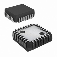
Manufacturer Part Number
TP3070V-XG
Description
IC COMBO II PCM FILTER 28PLCC
Manufacturer
National Semiconductor
Series
COMBO®IIr
Type
PCM Codec/Filterr
Datasheet
1.TP3070V-GNOPB.pdf
(26 pages)
Specifications of TP3070V-XG
Data Interface
PCM Audio Interface
Number Of Adcs / Dacs
1 / 1
Sigma Delta
No
Voltage - Supply, Analog
±5V
Voltage - Supply, Digital
±5V
Operating Temperature
-40°C ~ 85°C
Mounting Type
Surface Mount
Package / Case
28-LCC (J-Lead)
Lead Free Status / RoHS Status
Contains lead / RoHS non-compliant
Other names
*TP3070V-XG
Available stocks
Company
Part Number
Manufacturer
Quantity
Price
Company:

Part Number:
TP3070V-XG
Manufacturer:
NSC
Quantity:
5 510
Company:
Part Number:
TP3070V-XG
Manufacturer:
Texas Instruments
Quantity:
10 000
Part Number:
TP3070V-XG
Manufacturer:
NS/国半
Quantity:
20 000
Company:
Part Number:
TP3070V-XG/NOPB
Manufacturer:
Texas Instruments
Quantity:
10 000


Single Byte Power-Up/Down
Write Control Register
Read-Back Control Register
Write to Interface Latch Register
Read Interface Latch Register
Write Latch Direction Register
Read Latch Direction Register
Write Receive Gain Register
Read Receive Gain Register
Write Transmit Gain Register
Read Transmit Gain Register
Write Receive Time-Slot/Port
Read-Back Receive Time-Slot/Port
Write Transmit Time-Slot/Port
Read-Back Transmit Time-Slot/Port
Write Hybrid Balance Register 1
Read Hybrid Balance Register 1
Write Hybrid Balance Register 2
Read Hybrid Balance Register 2
Write Hybrid Balance Register 3
Read Hybrid Balance Register 3
Note 1: Bit 7 of bytes 1 and 2 is always the first bit clocked into or out from the CI, CO or CI/O pin. X = don’t care.
Note 2: “P” is the power-up/down control bit, see “Power-Up/Down Control” section. (“0” = Power Up, “1” = Power Down)
Note 3: Other register address codes are invalid and should not be used.
Functional Description
SERIAL CONTROL PORT
Control information and data are written into or read-back
from COMBO II via the serial control port consisting of the
control clock CCLK, the serial data input/output CI/O, (or
separate input, CI, and output, CO, on the TP3070 only), and
the Chip Select input, CS. All control instructions require 2
bytes, as listed in Table 1 , with the exception of a single byte
power-up/down command. The byte 1 bits are used as fol-
lows: bit 7 specifies power up or power down; bits 6, 5, 4 and
3 specify the register address; bit 2 specifies whether the in-
struction is read or write; bit 1 specifies a one or two byte in-
struction; and bit 0 is not used.
To shift control data into COMBO II, CCLK must be pulsed 8
times while CS is low. Data on the CI/O (or CI) input is
shifted into the serial input register on the falling edge of
each CCLK pulse. After all data is shifted in, the contents of
the input shift register are decoded, and may indicate that a
2nd byte of control data will follow. This second byte may ei-
ther be defined by a second byte-wide CS pulse or may fol-
low the first contiguously, i.e. it is not mandatory for CS to re-
turn high between the first and second control bytes. At the
end of CCLK8 in the 2nd control byte the data is loaded into
the appropriate programmable register. CS may remain low
continuously when programming successive registers, if de-
sired. However, CS should be set high when no data trans-
fers are in progress.
To readback Interface Latch data or status information from
COMBO II, the first byte of the appropriate instruction is
Function
TABLE 1. Programmable Register Instructions
(Continued)
7
P
P
P
P
P
P
P
P
P
P
P
P
P
P
P
P
P
P
P
P
P
6
X
0
0
0
0
0
0
0
0
0
0
1
1
1
1
0
0
0
0
1
1
Byte 1 (Note 1)
5
X
0
0
0
0
0
0
1
1
1
1
0
0
0
0
1
1
1
1
0
0
4
X
0
0
0
0
1
1
0
0
0
0
0
0
1
1
1
1
1
1
0
0
3
X
0
0
1
1
0
0
0
0
1
1
1
1
0
0
0
0
1
1
0
0
5
X
2
0
1
0
1
0
1
0
1
0
1
0
1
0
1
0
1
0
1
0
1
strobed in while CS is low, as defined in Table 1 . CS must be
kept low, or be taken low again for a further 8 CCLK cycles,
during which the data is shifted onto the CO or CI/O pin on
the rising edges of CCLK. When CS is high the CO or CI/O
pin is in the high-impedance TRI-STATE, enabling the CI/O
pins of many devices to be multiplexed together.
If CS returns high during either byte 1 or byte 2 before all
eight CCLK pulses of that byte occur, both the bit count and
byte count are reset and register contents are not affected.
This prevents loss of synchronization in the control interface
as well as corruption of register data due to processor inter-
rupt or other problem. When CS returns low again, the de-
vice will be ready to accept bit 1 of byte 1 of a new instruc-
tion.
Programmable Functions
1.0 POWER-UP/DOWN CONTROL
Following power-on initialization, power-up and power-down
control may be accomplished by writing any of the control in-
structions listed in Table 1 into COMBO II with the “P” bit set
to “0” for power-up or “1” for power-down. Normally it is rec-
ommended that all programmable functions be initially pro-
grammed while the device is powered down. Power state
control can then be included with the last programming in-
struction or the separate single-byte instruction. Any of the
programmable registers may also be modified while the de-
1
0
1
1
1
1
1
1
1
1
1
1
1
1
1
1
1
1
1
1
1
1
X
X
X
X
X
X
X
X
X
X
X
X
X
X
X
X
X
X
X
X
X
0
7
6
Byte 2 (Note 1)
5
See Table 2
See Table 2
See Table 4
See Table 4
See Table 3
See Table 3
See Table 8
See Table 8
See Table 7
See Table 7
See Table 6
See Table 6
See Table 6
See Table 6
Optimization
Derive from
TP3077SW
Routine in
Program
4
None
3
2
www.national.com
1
0
Related parts for TP3070V-XG
Image
Part Number
Description
Manufacturer
Datasheet
Request
R

Part Number:
Description:
IC INTERFAC PCM COMBO II 28-PLCC
Manufacturer:
National Semiconductor
Datasheet:

Part Number:
Description:
IC COMBO II EXT.TEMP. 28PLCC
Manufacturer:
National Semiconductor
Datasheet:

Part Number:
Description:
Audio CODEC IC
Manufacturer:
National Semiconductor
Datasheet:

Part Number:
Description:
Manufacturer:
National Semiconductor
Datasheet:
Part Number:
Description:
IC,PCM CODEC,SINGLE,CMOS,LDCC,28PIN,PLASTIC
Manufacturer:
National Semiconductor

Part Number:
Description:
Combo Ii Programmable Pcm Codec/filter
Manufacturer:
National Semiconductor Corporation
Datasheet:

Part Number:
Description:
TRISILTM
Manufacturer:
STMicroelectronics
Datasheet:
Part Number:
Description:
National Semiconductor [8-Bit D/A Converter]
Manufacturer:
National Semiconductor
Datasheet:
Part Number:
Description:
National Semiconductor [Media Coprocessor]
Manufacturer:
National Semiconductor
Datasheet:
Part Number:
Description:
Digitally Controlled Tone and Volume Circuit with Stereo Audio Power Amplifier, Microphone Preamp Stage and National 3D Sound
Manufacturer:
National Semiconductor
Datasheet: