TP3070V-XG National Semiconductor, TP3070V-XG Datasheet - Page 22
TP3070V-XG
Manufacturer Part Number
TP3070V-XG
Description
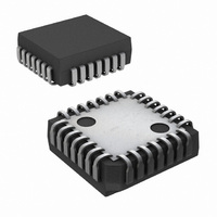
IC COMBO II PCM FILTER 28PLCC
Manufacturer
National Semiconductor
Series
COMBO®IIr
Type
PCM Codec/Filterr
Datasheet
1.TP3070V-GNOPB.pdf
(26 pages)
Specifications of TP3070V-XG
Data Interface
PCM Audio Interface
Number Of Adcs / Dacs
1 / 1
Sigma Delta
No
Voltage - Supply, Analog
±5V
Voltage - Supply, Digital
±5V
Operating Temperature
-40°C ~ 85°C
Mounting Type
Surface Mount
Package / Case
28-LCC (J-Lead)
Lead Free Status / RoHS Status
Contains lead / RoHS non-compliant
Other names
*TP3070V-XG
Available stocks
Company
Part Number
Manufacturer
Quantity
Price
Company:

Part Number:
TP3070V-XG
Manufacturer:
NSC
Quantity:
5 510
Company:
Part Number:
TP3070V-XG
Manufacturer:
Texas Instruments
Quantity:
10 000
Part Number:
TP3070V-XG
Manufacturer:
NS/国半
Quantity:
20 000
Company:
Part Number:
TP3070V-XG/NOPB
Manufacturer:
Texas Instruments
Quantity:
10 000


www.national.com
Definitions and Timing Conventions
DEFINITIONS
V
V
V
V
Threshold Region The threshold region is the range of in-
Valid Signal
Invalid signal
TIMING CONVENTIONS
For the purposes of this timing specification the following
conventions apply.
Input Signals
Period
Rise Time
Fall Time
Pulse Width High The high pulse width width is designated
IH
IL
OH
OL
All input signals may be characterized
as: V
10 ns.
The period of the clock signal is desig-
nated as t
mnemonic of the clock signal being
specified.
Rise times are designated as t
yy represents a mnemonic of the signal
whose rise time is being specified. t
measured from V
Fall times are designated as t
yy represents a mnemonic of the signal
whose fall time is being specified. t
measured from V
as t
monic of the input or output signal whose
pulse width is being specified. High
V
an input level is guaranteed to appear as
a logical one. This parameter is to be
measured by performing a functional
test at reduced clock speeds and nomi-
nal timing, (i.e., not minimum setup and
hold times or output strobes), with the
high level of all driving signals set to V
and maximum supply voltages applied
to the device.
V
an input level is guaranteed to appear as
a logical zero to the device. This param-
eter is measured in the same manner as
V
set to V
applied to the device.
V
which an output placed in a logical one
state will converge when loaded at the
maximum specified load current.
V
which an output placed in a logical zero
state will converge when loaded at the
maximum specified load current.
put voltages between V
A signal is Valid if it is in one of the valid
logic states. (i.e., above V
V
deemed valid at the instant it enters a
valid state.
A signal is invalid if it is not in a valid
logic state, i.e., when it is in the thresh-
old region between V
specifications, a signal is deemed In-
valid at the instant it enters the threshold
region.
IH
IL
IH
OH
OL
IL
). In timing specifications, a signal is
WzzH
is the D.C. input level below which
but with all driving signal low levels
is the D.C. input level above which
is the maximum D.C. output level to
L
is the minimum D.C. output level to
= 0.4V, V
IL
, where zz represents the mne-
and minimum supply voltages
Pxx
where
H
IL
IH
= 2.4V, t
to V
to V
IL
xx
and V
IH
IL
IL
represents the
.
.
R
and V
<
IH
IH
Ryy
Fyy
10 ns, t
. In timing
or below
IH
, where
, where
.
Ryy
Fyy
F
IH
<
is
is
22
Pulse Width Low
Setup Time
Hold Time
Delay Time
pulse widths are measured from V
V
The low pulse width is designated as
t
monic of the input or output signal whose
pulse width is being specified. Low pulse
widths are measured from V
Setup times are designated as t
where ww represents the mnemonic of
the input signal whose setup time is be-
ing specified relative to a clock or strobe
input represented by mnemonic xx.
Setup times are measured from the ww
Valid to xx Invalid.
Hold times are designated as T
where ww represents the mnemonic of
the input signal whose hold time is being
specified relative to a clock or strobe in-
put represented by the mnemonic xx.
Hold times are measured from xx Valid
to ww Invalid.
Delay
T
mnemonic of the input reference signal
and yy represents the mnemonic of the
output signal whose timing is being
specified relative to xx. The mnemonic
may optionally be terminated by an H or
L to specify the high going or low going
transition of the output signal. Maximum
delay times are measured from xx Valid
to yy Valid. Minimum delay times are
measured from xx Valid to yy Invalid.
This parameter is tested under the load
conditions specified in the Conditions
column of the Timing Specifications sec-
tion of this datasheet.
WzzL
Dxxyy
IH
.
, where zz represents the mne-
[ IHIL], where xx represents the
times
are
designated
IL
to V
Hwwxx
Swwxx
IL
IH
.
as
to
,
,
Related parts for TP3070V-XG
Image
Part Number
Description
Manufacturer
Datasheet
Request
R

Part Number:
Description:
IC INTERFAC PCM COMBO II 28-PLCC
Manufacturer:
National Semiconductor
Datasheet:

Part Number:
Description:
IC COMBO II EXT.TEMP. 28PLCC
Manufacturer:
National Semiconductor
Datasheet:

Part Number:
Description:
Audio CODEC IC
Manufacturer:
National Semiconductor
Datasheet:

Part Number:
Description:
Manufacturer:
National Semiconductor
Datasheet:
Part Number:
Description:
IC,PCM CODEC,SINGLE,CMOS,LDCC,28PIN,PLASTIC
Manufacturer:
National Semiconductor

Part Number:
Description:
Combo Ii Programmable Pcm Codec/filter
Manufacturer:
National Semiconductor Corporation
Datasheet:

Part Number:
Description:
TRISILTM
Manufacturer:
STMicroelectronics
Datasheet:
Part Number:
Description:
National Semiconductor [8-Bit D/A Converter]
Manufacturer:
National Semiconductor
Datasheet:
Part Number:
Description:
National Semiconductor [Media Coprocessor]
Manufacturer:
National Semiconductor
Datasheet:
Part Number:
Description:
Digitally Controlled Tone and Volume Circuit with Stereo Audio Power Amplifier, Microphone Preamp Stage and National 3D Sound
Manufacturer:
National Semiconductor
Datasheet: