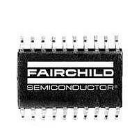
RC5051M Fairchild Semiconductor, RC5051M Datasheet - Page 10

RC5051M
Manufacturer Part Number
RC5051M
Description
DC/DC Switching Controllers DC-DC Converter Prog Sync
Manufacturer
Fairchild Semiconductor
Datasheet
1.RC5051M.pdf
(16 pages)
Specifications of RC5051M
Number Of Outputs
1
Output Voltage
1.3 V to 3.5 V
Output Current
15 A
Mounting Style
SMD/SMT
Package / Case
SOIC-20 Wide
Maximum Operating Temperature
+ 70 C
Minimum Operating Temperature
0 C
Lead Free Status / Rohs Status
Lead free / RoHS Compliant
Available stocks
Company
Part Number
Manufacturer
Quantity
Price
Part Number:
RC5051M
Manufacturer:
RAYTHEON
Quantity:
20 000
Part Number:
RC5051M-T
Manufacturer:
FAIRCHILD/仙童
Quantity:
20 000
Part Number:
RC5051MA
Manufacturer:
FAIRCHILD/仙童
Quantity:
20 000
RC5051
Application Information
The RC5051 Controller
The RC5051 is a programmable synchronous DC-DC con-
troller IC. When designed around the appropriate external
components, the RC5051 can be configured to deliver more
than 19A of output current, as appropriate for the Klamath
and Deschutes and other processors. The RC5051 functions
as a fixed frequency PWM step down regulator.
Main Control Loop
Refer to the RC5051 Block Diagram on page 1. The RC5051
implements “summing mode control”, which is different
from both classical voltage-mode and current-mode control.
It provides superior performance to either by allowing a
large converter bandwidth over a wide range of output loads.
The control loop of the regulator contains two main sections:
the analog control block and the digital control block. The
analog section consists of signal conditioning amplifiers
feeding into a set of comparators which provide the inputs to
the digital control block. The signal conditioning section
accepts inputs from the IFB (current feedback) and VFB
(voltage feedback) pins and sets up two controlling signal
paths. The first, the voltage control path, amplifies the differ-
ence between the VFB signal the reference voltage from the
DAC and presents the output to one of the summing ampli-
fier inputs. The second, current control path, takes the differ-
ence between the IFB and VFB pins and presents the
resulting signal to another input of the summing amplifier.
These two signals are then summed together with the slope
compensation input from the oscillator. This output is then
presented to a comparator, which provides the main PWM
control signal to the digital control block.
The digital control block takes the analog comparator inputs
and the main clock signal from the oscillator to provide the
appropriate pulses to the HIDRV and LODRV output pins.
These two outputs control the external power MOSFETs.
The digital block utilizes high speed Schottky transistor
logic, allowing the RC5051 to operate at clock speeds as
high as 1MHz.
There are additional comparators in the analog control sec-
tion whose function is to set the point at which the RC5051
enters its pulse skipping mode during light loads, as well as
the point at which the current limit comparator disables the
output drive signals to the external power MOSFETs.
High Current Output Drivers
The RC5051 contains two identical high current output
drivers that utilize high speed bipolar transistors in a push-
pull configuration. The drivers’ power and ground are sepa-
rated from the chip’s power and ground for switching noise
immunity. The HIDRV driver has a power supply pin,
10
VCCQP, which is supplied from an external 12V source
through a series resistor or from a charge-pump circuit
powered from 5V if 12V is not available. The LODRV driver
has a power supply pin, VCCP, which can be supplied from
either the 12V or 5V source. The resulting voltages are suffi-
cient to provide the gate to source drive to the external
MOSFETs required in order to achieve a low R
Internal Voltage Reference
The reference included in the RC5051 is a precision band-
gap voltage reference. Its internal resistors are precisely
trimmed to provide a near zero temperature coefficient (TC).
Based on the reference is the output from an integrated 5-bit
DAC. The DAC monitors the 5 voltage identification pins,
VID0–VID4. When the VID4 pin is at logic HIGH, the DAC
scales the reference voltage from 2.0V to 3.5V in 100mV
increments. When VID4 is pulled LOW, the DAC scales the
reference from 1.30V to 2.05V in 50mV increments. All VID
codes are available, including those below 1.80V. For guar-
anteed stable operation under all loading conditions, 0.1µF
of decoupling capacitance should be connected to the VREF
pin. No load should be connected to VREF.
Power Good (PWRGD)
The RC5051 Power Good function is designed in accordance
with the Pentium II DC-DC converter specifications and
provides a continuous voltage monitor on the VFB pin. The
circuit compares the VFB signal to the VREF voltage and
outputs an active-low interrupt signal to the CPU should the
power supply voltage deviate more than 12% of its nominal
setpoint. The Power Good flag provides no other control
function to the RC5051.
Output Enable (ENABLE)
The RC5051 will accept an open collector/TTL signal for
controlling the output voltage. The low state disables the out-
put voltage. When disabled, the PWRGD output is in the low
state. If an enable is not required in the circuit, this pin may
be left open.
Over-Voltage Protection
The RC5051 constantly monitors the output voltage for pro-
tection against over voltage conditions. If the voltage at the
VFB pin exceeds 20% of the selected program voltage, an
over-voltage condition is assumed and the RC5051 disables
the output drive signal to the external MOSFETs. The DC-
DC converter returns to normal operation after the fault has
been removed.
Over-Current Protection
Current sense is implemented in the RC5051 to reduce the
duty cycle of the output drive signal to the MOSFETs when
an over-current condition is detected. The voltage drop
created by the output current flowing across a sense resistor
is presented to an internal comparator. When the voltage
PRODUCT SPECIFICATION
REV. 1.0.4 4/2/01
DS,ON
.


