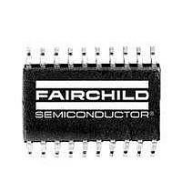
RC5051M Fairchild Semiconductor, RC5051M Datasheet - Page 3

RC5051M
Manufacturer Part Number
RC5051M
Description
DC/DC Switching Controllers DC-DC Converter Prog Sync
Manufacturer
Fairchild Semiconductor
Datasheet
1.RC5051M.pdf
(16 pages)
Specifications of RC5051M
Number Of Outputs
1
Output Voltage
1.3 V to 3.5 V
Output Current
15 A
Mounting Style
SMD/SMT
Package / Case
SOIC-20 Wide
Maximum Operating Temperature
+ 70 C
Minimum Operating Temperature
0 C
Lead Free Status / Rohs Status
Lead free / RoHS Compliant
Available stocks
Company
Part Number
Manufacturer
Quantity
Price
Part Number:
RC5051M
Manufacturer:
RAYTHEON
Quantity:
20 000
Part Number:
RC5051M-T
Manufacturer:
FAIRCHILD/仙童
Quantity:
20 000
Part Number:
RC5051MA
Manufacturer:
FAIRCHILD/仙童
Quantity:
20 000
PRODUCT SPECIFICATION
Absolute Maximum Ratings
Operating Conditions
Electrical Specifications
(V
The denotes specifications which apply over the full operating temperature range.
Notes:
1. Steady Date Voltage Regulation includes Initial Voltage Setpoint, Load Regulation, Output Ripple and Output Temperature Drift
2. As measured at the converter’s output capacitors. For motherboard applications, the PCB layout should exhibit no more than
REV. 1.0.4 4/2/01
Supply Voltages, VCCA, VCCP, VCCQP to GND
Supply Voltage VCCQP, Charge Pump (V
Voltage Identification Code Inputs, VID4-VID0
Junction Temperature, T
Storage Temperature
Lead Soldering Temperature, 10 seconds
Parameter
Supply Voltage, VCCA, VCCP
Input Logic HIGH
Input Logic LOW
Ambient Operating Temp
Output Driver Supply, VCCQP
PWRGD threshold
Parameter
Output Voltage
Output Current
Initial Voltage Setpoint
Output Temperature Drift
Load Regulation
Line Regulation
Output Ripple
Total Output Variation
Total Output Variation
Short Circuit Detect Threshold
Efficiency
Output Driver Rise and Fall Time
Output Driver Deadtime 1
Output Driver Deadtime 2
Turn-on Response Time
Oscillator Range
Oscillator Frequency
Max Duty Cycle
CCA
and is measured at the converter’s output capacitors.
0.5m trace resistance between the converter’s output capacitors and the CPU.
Steady State
Transient
= 5V, V
2
OUT
1
= 2.8V, f
J
osc
= 300 KHz, and T
Conditions
See Table 1
I
I
V
20MHz BW, I
V
V
I
I
I
C
T
See Figure 2
See Figure 2
See Figure 2
LOAD
LOAD
LOAD
LOAD
LOAD
A
IN
OUT
OUT
EXT
= 0 to 70 C V
= 4.75V to 5.25V
Logic High
Logic Low
Conditions
IN
= 100 pF
= 2.8V
= 2.0V
= 14.2A, V
= 0.8A, V
= 0.8A to 14.2A
= 0.8 to 14.2A, V
= 0A to 14.2A
+VCCA)
A
= +25 C using circuit in Figure 1, unless otherwise noted)
LOAD
V
V
OUT
OUT
OUT
OUT
OUT
= 14.2A
= 2.8V
= 2.0V
V
= 2.8V
= 2.8V
= 2.0V
OUT
OUT
= 2.8V
= 2.0V
Min.
4.75
2.0
8.5
93
88
0
2.797
2.000
2.740
1.940
2.670
1.900
Min.
100
270
1.3
80
90
Typ.
5
2.825
2.020
Typ.
+16
+11
120
300
-20
15
82
80
80
95
13
5
2
-65 to 150 C
Max.
5.25
150 C
107
112
300 C
0.8
70
12
2.853
2.040
2.900
2.060
2.930
2.100
13V
18V
13V
Max.
1000
140
330
3.5
10
%V
%V
%/f
Units
Units
mVpk
RC5051
msec
nsec
nsec
KHz
KHz
mV
mV
mV
mV
mV
V
V
V
V
OUT
OUT
C
%
%
V
A
V
V
V
V
V
V
OSC
3


