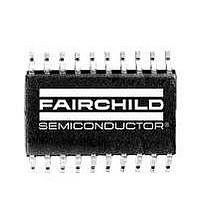
RC5051M Fairchild Semiconductor, RC5051M Datasheet - Page 12

RC5051M
Manufacturer Part Number
RC5051M
Description
DC/DC Switching Controllers DC-DC Converter Prog Sync
Manufacturer
Fairchild Semiconductor
Datasheet
1.RC5051M.pdf
(16 pages)
Specifications of RC5051M
Number Of Outputs
1
Output Voltage
1.3 V to 3.5 V
Output Current
15 A
Mounting Style
SMD/SMT
Package / Case
SOIC-20 Wide
Maximum Operating Temperature
+ 70 C
Minimum Operating Temperature
0 C
Lead Free Status / Rohs Status
Lead free / RoHS Compliant
Available stocks
Company
Part Number
Manufacturer
Quantity
Price
Part Number:
RC5051M
Manufacturer:
RAYTHEON
Quantity:
20 000
Part Number:
RC5051M-T
Manufacturer:
FAIRCHILD/仙童
Quantity:
20 000
Part Number:
RC5051MA
Manufacturer:
FAIRCHILD/仙童
Quantity:
20 000
RC5051
Inductor Selection
Choosing the value of the inductor is a tradeoff between
allowable ripple voltage and required transient response. The
system designer can choose any value within the allowed
minimum to maximum range in order to either minimize rip-
ple or maximize transient performance. The first order equa-
tion (close approximation) for minimum inductance is:
where:
V
V
f = DC/DC converter switching frequency
ESR = Equivalent series resistance of all output capacitors in
parallel
V
budget.
The first order equation for maximum allowed inductance is:
where:
C
I
V
transient
D
(usually 95%).
Some margin should be maintained away from both L
and L
adds expense since all the variables are predetermined by
system performance except for C
to increase L. Adding margin by decreasing L can either be
done by purchasing capacitors with lower ESR or by increas-
ing the DC/DC converter switching frequency. The RC5051
12
L
L
pp
out
in
o
min
ripple
max
tb
m
= Maximum to minimum load transient current
PWM/PFM
= Input Power Supply
= The total output capacitance
= The output voltage tolerance budget allocated to load
= Maximum duty cycle for the DC/DC converter
= Output Voltage
Control
max
=
=
= Maximum peak to peak output ripple voltage
------------------------------
2C
. Adding margin by increasing L almost always
V
in
Figure 4. Gate Bias Configuration
O
–
f
V
----------------------------------------------- -
V
out
+12V
in
VCCQP
GNDP
LODRV
–
HIDRV
V
V
---------- -
I
V
out
2
PP
out
in
D
47
1 F
m
---------------- -
V
o
V
ESR
ripple
, which must be increased
tb
D1
Q1
Q2
L2
+5V
D2
RS
65-5051-07
C
OUT
min
VO
is capable of running at high switching frequencies and
provides significant cost savings for the newer CPU systems
that typically run at high supply current.
RC5051 Short Circuit Current Characteristics
The RC5051 short circuit current characteristic includes a
hysteresis function that prevents the DC-DC converter from
oscillating in the event of a short circuit. Figure 5 shows the
typical characteristic of the DC-DC converter circuit with a
6.8 m sense resistor. The converter exhibits a normal load
regulation characteristic until the voltage across the resistor
exceeds the internal short circuit threshold of 120mV
(= 17.5A * 6.8m ). At this point, the internal comparator
trips and signals the controller to reduce the converter’s duty
cycle to approximately 20%. This causes a drastic reduction
in the output voltage as the load regulation collapses into the
short circuit control mode. With a 40m output short, the
voltage is reduced to 15A * 40m = 600mV. The output
voltage does not return to its nominal value until the output
current is reduced to a value within the safe operating range
for the DC-DC converter.
Schottky Diode Selection
The application circuit of Figure 1 shows a Schottky diode,
D2, which is used as a free-wheeling diode to assure that the
body-diode in Q2 does not conduct when the upper
MOSFET is turning off and the lower MOSFET is turning
on. It is undesirable for this diode to conduct because its high
forward voltage drop and long reverse recovery time
degrades efficiency, and so the Schottky provides a shunt
path for the current. Since this time duration is very short,
the selection criterion for the diode is that the forward volt-
age of the Schottky at the output current should be less than
the forward voltage of the MOSFET’s body diode.
Output Filter Capacitors
The output bulk capacitors of a converter help determine its
output ripple voltage and its transient response. It has
already been seen in the section on selecting an inductor that
the ESR helps set the minimum inductance, and the capaci-
tance value helps set the maximum inductance. For most
converters, however, the number of capacitors required is
3.5
3.0
2.5
2.0
1.5
1.0
0.5
Figure 5. RC5051 Short Circuit Characteristic
0
0
Output Voltage vs. Output Current
5
Output Current (A)
RSENSE = 6m
10
PRODUCT SPECIFICATION
15
REV. 1.0.4 4/2/01
20
25


