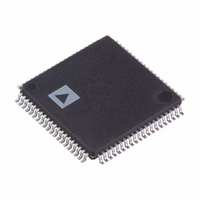
AD9883AKSTZ-140 Analog Devices Inc, AD9883AKSTZ-140 Datasheet - Page 11

AD9883AKSTZ-140
Manufacturer Part Number
AD9883AKSTZ-140
Description
IC FLAT PANEL INTERFACE 80-LQFP
Manufacturer
Analog Devices Inc
Datasheet
1.AD9883AKSTZ-140.pdf
(28 pages)
Specifications of AD9883AKSTZ-140
Applications
Displays, Monitors, TV
Interface
Analog
Voltage - Supply
3 V ~ 3.6 V
Package / Case
80-LQFP
Mounting Type
Surface Mount
Lead Free Status / RoHS Status
Lead free / RoHS Compliant
Available stocks
Company
Part Number
Manufacturer
Quantity
Price
Company:
Part Number:
AD9883AKSTZ-140
Manufacturer:
Analog Devices Inc
Quantity:
135
Company:
Part Number:
AD9883AKSTZ-140
Manufacturer:
ADI
Quantity:
455
Company:
Part Number:
AD9883AKSTZ-140
Manufacturer:
Analog Devices Inc
Quantity:
10 000
Part Number:
AD9883AKSTZ-140
Manufacturer:
ADI/亚德诺
Quantity:
20 000
Gain and Offset Control
The AD9883A can accommodate input signals with inputs
ranging from 0.5 V to 1.0 V full scale. The full-scale range is set
in three 8-bit registers (Red Gain, Green Gain, and Blue Gain).
Note that increasing the gain setting results in an image with
less contrast.
The offset control shifts the entire input range, resulting in a
change in image brightness. Three 7-bit registers (Red Offset,
Green Offset, Blue Offset) provide independent settings for
each channel. The offset controls provide a ± 63 LSB adjust-
ment range. This range is connected with the full-scale range, so
if the input range is doubled (from 0.5 V to 1.0 V) then the offset
step size is also doubled (from 2 mV per step to 4 mV per step).
Figure 2 illustrates the interaction of gain and offset controls.
The magnitude of an LSB in offset adjustment is proportional
to the full-scale range, so changing the full-scale range also
changes the offset. The change is minimal if the offset setting is
near midscale. When changing the offset, the full-scale range is
not affected, but the full-scale level is shifted by the same amount
as the zero scale level.
Sync-on-Green
The Sync-on-Green input operates in two steps. First, it sets a
baseline clamp level off of the incoming video signal with a
negative peak detector. Second, it sets the sync trigger level to a
programmable level (typically 150 mV) above the negative peak.
The Sync-on-Green input must be ac-coupled to the Green
analog input through its own capacitor, as shown in Figure 3.
The value of the capacitor must be 1 nF ± 20%. If Sync-on-Green
is not used, this connection is not required. Note that the Sync-
on-Green signal is always negative polarity.
REV. B
1.0
0.5
0.
0
00H
Figure 3. Typical Clamp Configuration
Figure 2. Gain and Offset Control
47nF
47nF
47nF
1nF
GAIN
R
B
G
SOG
AIN
AIN
AIN
OFFSET = 7FH
OFFSET = 3FH
OFFSET = 00H
OFFSET = 7FH
OFFSET = 3FH
OFFSET = 00H
FFH
–11–
Clock Generation
A phase locked loop (PLL) is employed to generate the pixel
clock. In this PLL, the Hsync input provides a reference fre-
quency. A voltage controlled oscillator (VCO) generates a much
higher pixel clock frequency. This pixel clock is divided by the
PLL divide value (registers 01H and 02H) and phase compared
with the Hsync input. Any error is used to shift the VCO fre-
quency and maintain lock between the two signals.
The stability of this clock is a very important element in provid-
ing the clearest and most stable image. During each pixel time,
there is a period during which the signal is slewing from the old
pixel amplitude and settling at its new value. Then there is a
time when the input voltage is stable, before the signal must
slew to a new value (Figure 4). The ratio of the slewing time to
the stable time is a function of the bandwidth of the graphics
DAC and the bandwidth of the transmission system (cable and
termination). It is also a function of the overall pixel rate. Clearly,
if the dynamic characteristics of the system remain fixed, the
slewing and settling time is likewise fixed. This time must be
subtracted from the total pixel period, leaving the stable period.
At higher pixel frequencies, the total cycle time is shorter, and the
stable pixel time becomes shorter as well.
Any jitter in the clock reduces the precision with which the
sampling time can be determined, and must also be subtracted
from the stable pixel time.
Considerable care has been taken in the design of the AD9883A’s
clock generation circuit to minimize jitter. As indicated in
Figure 5, the clock jitter of the AD9883A is less than 5% of the
total pixel time in all operating modes, making the reduction in
the valid sampling time due to jitter negligible.
14
12
10
8
6
4
2
0
Figure 5. Pixel Clock Jitter vs. Frequency
PIXEL CLOCK
0
31.5 36.0 36.0 50.0 56.25
Figure 4. Pixel Sampling Times
INVALID SAMPLE TIMES
FREQUENCY – MHz
75.0 85.5
AD9883A
110.0


