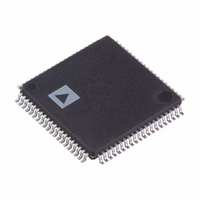
AD9883AKSTZ-140 Analog Devices Inc, AD9883AKSTZ-140 Datasheet - Page 18

AD9883AKSTZ-140
Manufacturer Part Number
AD9883AKSTZ-140
Description
IC FLAT PANEL INTERFACE 80-LQFP
Manufacturer
Analog Devices Inc
Datasheet
1.AD9883AKSTZ-140.pdf
(28 pages)
Specifications of AD9883AKSTZ-140
Applications
Displays, Monitors, TV
Interface
Analog
Voltage - Supply
3 V ~ 3.6 V
Package / Case
80-LQFP
Mounting Type
Surface Mount
Lead Free Status / RoHS Status
Lead free / RoHS Compliant
Available stocks
Company
Part Number
Manufacturer
Quantity
Price
Company:
Part Number:
AD9883AKSTZ-140
Manufacturer:
Analog Devices Inc
Quantity:
135
Company:
Part Number:
AD9883AKSTZ-140
Manufacturer:
ADI
Quantity:
455
Company:
Part Number:
AD9883AKSTZ-140
Manufacturer:
Analog Devices Inc
Quantity:
10 000
Part Number:
AD9883AKSTZ-140
Manufacturer:
ADI/亚德诺
Quantity:
20 000
AD9883A
04
CLAMP TIMING
05
06
Hsync PULSEWIDTH
07
INPUT GAIN
08
09
0A
7–0 Clamp Placement
7–0 Hsync Output Pulsewidth
7–0 Red Channel Gain Adjust
7–3 Clock Phase Adjust
A 5-bit value that adjusts the sampling phase in 32 steps
across one pixel time. Each step represents an 11.25° shift
in sampling phase.
The power-up default value is 16.
An 8-bit register that sets the position of the internally
generated clamp.
When Clamp Function (Register 0FH, Bit 7) = 0, a clamp
signal is generated internally, at a position established by
the clamp placement and for a duration set by the clamp
duration. Clamping is started (Clamp Placement) pixel
periods after the trailing edge of Hsync. The clamp placement
may be programmed to any value between 1 and 255.
The clamp should be placed during a time that the input
signal presents a stable black-level reference, usually the
back porch period between Hsync and the image.
When Clamp Function = 1, this register is ignored.
7–0 Clamp Duration
An 8-bit register that sets the duration of the internally
generated clamp.
For the best results, the clamp duration should be set to
include the majority of the black reference signal time that
follows the Hsync signal trailing edge. Insufficient clamping
time can produce brightness changes at the top of the screen,
and a slow recovery from large changes in the average picture
level (APL), or brightness.
When Clamp Function = 1, this register is ignored.
An 8-bit register that sets the duration of the Hsync
output pulse.
The leading edge of the Hsync output is triggered by the
internally generated, phase-adjusted PLL feedback clock.
The AD9883A then counts a number of pixel clocks equal
to the value in this register. This triggers the trailing edge
of the Hsync output, which is also phase adjusted.
An 8-bit word that sets the gain of the Red channel.
The AD9883A can accommodate input signals with a
full-scale range of between 0.5 V and 1.0 V p-p. Setting
REDGAIN to 255 corresponds to a 1.0 V input range.
A REDGAIN of 0 establishes a 0.5 V input range. Note
that increasing REDGAIN results in the picture having less
contrast (the input signal uses fewer of the available
converter codes). See Figure 2.
7–0 Green Channel Gain Adjust
An 8-bit word that sets the gain of the Green channel. See
REDGAIN (08).
7–0 Blue Channel Gain Adjust
An 8-bit word that sets the gain of the Blue channel. See
REDGAIN (08).
–18–
INPUT OFFSET
0B
0C
0D
MODE CONTROL 1
0E
0E
7–1 Red Channel Offset Adjust
A 7-bit offset binary word that sets the dc offset of the Red
channel. One LSB of offset adjustment equals approximately
one LSB change in the ADC offset. Therefore, the absolute
magnitude of the offset adjustment scales as the gain of the
channel is changed. A nominal setting of 63 results in the
channel nominally clamping the back porch (during the
clamping interval) to Code 00. An offset setting of 127 results
in the channel clamping to Code 64 of the ADC. An offset
setting of 0 clamps to Code –63 (off the bottom of the
range). Increasing the value of Red Offset decreases the
brightness of the channel.
7–1 Green Channel Offset Adjust
A 7-bit offset binary word that sets the dc offset of the
Green channel. See REDOFST (0B).
7–1 Blue Channel Offset Adjust
A 7-bit offset binary word that sets the dc offset of the
Green channel. See REDOFST (0B).
7 Hsync Input Polarity Override
This register is used to override the internal circuitry
that determines the polarity of the Hsync signal going
into the PLL.
Override Bit
0
1
The default for Hsync polarity override is 0 (polarity
determined by chip).
6 HSPOL Hsync Input Polarity
A bit that must be set to indicate the polarity of the
Hsync signal that is applied to the PLL Hsync input.
HSPOL
0
1
Active Low means the leading edge of the Hsync pulse
is negative going. All timing is based on the leading edge
of Hsync, which is the falling edge. The rising edge has no
effect.
Active high is inverted from the traditional Hsync, with
a positive-going pulse. This means that timing will be
based on the leading edge of Hsync, which is now the
rising edge.
The device will operate if this bit is set incorrectly, but the
internally generated clamp position, as established by
Clamp Placement (Register 05H), will not be placed as
expected, which may generate clamping errors.
The power-up default value is HSPOL = 1.
Table IX. Hsync Input Polarity Override Settings
Table X. Hsync Input Polarity Settings
Function
Active Low
Active High
Function
Hsync Polarity Determined by Chip
Hsync Polarity Determined by User
REV. B


