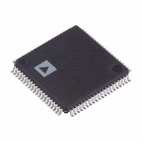
AD9883AKSTZ-140 Analog Devices Inc, AD9883AKSTZ-140 Datasheet - Page 21

AD9883AKSTZ-140
Manufacturer Part Number
AD9883AKSTZ-140
Description
IC FLAT PANEL INTERFACE 80-LQFP
Manufacturer
Analog Devices Inc
Datasheet
1.AD9883AKSTZ-140.pdf
(28 pages)
Specifications of AD9883AKSTZ-140
Applications
Displays, Monitors, TV
Interface
Analog
Voltage - Supply
3 V ~ 3.6 V
Package / Case
80-LQFP
Mounting Type
Surface Mount
Lead Free Status / RoHS Status
Lead free / RoHS Compliant
Available stocks
Company
Part Number
Manufacturer
Quantity
Price
Company:
Part Number:
AD9883AKSTZ-140
Manufacturer:
Analog Devices Inc
Quantity:
135
Company:
Part Number:
AD9883AKSTZ-140
Manufacturer:
ADI
Quantity:
455
Company:
Part Number:
AD9883AKSTZ-140
Manufacturer:
Analog Devices Inc
Quantity:
10 000
Part Number:
AD9883AKSTZ-140
Manufacturer:
ADI/亚德诺
Quantity:
20 000
13
14
14
14
14
REV. B
7–0 Post-Coast
This register allows the coast signal to be applied follow-
ing the Vsync signal. This is necessary in cases where
post-equalization pulses are present. The step size for this
control is one Hsync period.
The default is 0.
7 Hsync Detect
This bit is used to indicate when activity is detected on
the Hsync input pin (Pin 30). If Hsync is held high or
low, activity will not be detected.
Detect
0
1
The sync processing block diagram shows where this
function is implemented.
6 AHS – Active Hsync
This bit indicates which Hsync input source is being used
by the PLL (Hsync input or Sync-on-Green). Bits 7 and 1
in this register determine which source is used. If both
Hsync and SOG are detected, the user can determine which
has priority via Bit 3 in register 0EH. The user can override
this function via Bit 4 in register 0EH. If the override bit
is set to Logic 1, then this bit will be forced to whatever
the state of Bit 3 in register 0EH is set to.
Bit 7
(Hsync
Detect)
0
0
1
1
X
AHS = 0 means use the Hsync pin input for Hsync.
AHS = 1 means use the SOG pin input for Hsync.
The override bit is in register 0EH, Bit 4.
5 Detected Hsync Input Polarity Status
This bit reports the status of the Hsync input polarity
detection circuit. It can be used to determine the polarity
of the Hsync input. The detection circuit’s location is
shown in the Sync Processing Block Diagram (Figure 12).
Table XXIX. Detected Hsync Input Polarity Status
Hsync Polarity Status
0
1
4 Vsync Detect
This bit is used to indicate when activity is detected on
the Vsync input pin (Pin 31). If Vsync is held steady high
or low, activity will not be detected.
Table XXVII. Hsync Detection Results
Table XXVIII. Active Hsync Results
Bit 1
(SOG
Detect)
0
1
0
1
X
Function
No Activity Detected
Activity Detected
Bit 4,
Reg 0EH
(Override)
0
0
0
0
1
Result
Negative
Positive
AHS
Bit 3 in 0EH
1
0
Bit 3 in 0EH
Bit 3 in 0EH
–21–
14
14
14
14
Detect
0
1
The Sync Processing Block Diagram (Figure 12) shows
where this function is implemented.
3 AVS – Active Vsync
This bit indicates which Vsync source is being used: the
Vsync input or output from the sync separator. Bit 4 in this
register determines which is active. If both Vsync and
SOG are detected, the user can determine which has
priority via Bit 0 in register 0EH. The user can override this
function via Bit 1 in register 0EH. If the override bit is set
to Logic 1, this bit will be forced to whatever the state of Bit 0
in register 0EH is set.
AVS = 0 means Vsync input.
AVS = 1 means Sync separator.
The override bit is in register 0EH, Bit 1.
2
This bit reports the status of the Vsync output polarity
detection circuit. It can be used to determine the polarity
of the Vsync output. The detection circuit’s location is-
shown in the Sync Processing Block Diagram (Figure 12).
Vsync Polarity Status
0
1
1
This bit is used to indicate when sync activity is detected
on the Sync-on-Green input pin (Pin 49).
Detect
0
1
The Sync Processing Block Diagram (Figure 12) shows
where this function is implemented.
0
This bit reports the status of the Coast input polarity
detection circuit. It can be used to determine the polarity
of the Coast input. The detection circuit’s location is shown
in the Sync Processing Block Diagram (Figure 12).
Bit 4, Reg 14H
(Vsync Detect)
1
0
X
Table XXXII. Detected Vsync Output Polarity Status
Table XXXIII. Sync-on-Green Detection Results
Detected Vsync Output Polarity Status
Detected Coast Polarity Status
Sync-on-Green Detect
Table XXX. Vsync Detection Results
Table XXXI. Active Vsync Results
Function
No Activity Detected
Activity Detected
Function
No Activity Detected
Activity Detected
Bit 1, Reg 0EH
(Override)
0
0
1
Result
Active Low
Active High
AD9883A
AVS
0
1
Bit 0 in 0EH


