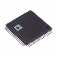
AD9883AKSTZ-140 Analog Devices Inc, AD9883AKSTZ-140 Datasheet - Page 23

AD9883AKSTZ-140
Manufacturer Part Number
AD9883AKSTZ-140
Description
IC FLAT PANEL INTERFACE 80-LQFP
Manufacturer
Analog Devices Inc
Datasheet
1.AD9883AKSTZ-140.pdf
(28 pages)
Specifications of AD9883AKSTZ-140
Applications
Displays, Monitors, TV
Interface
Analog
Voltage - Supply
3 V ~ 3.6 V
Package / Case
80-LQFP
Mounting Type
Surface Mount
Lead Free Status / RoHS Status
Lead free / RoHS Compliant
Available stocks
Company
Part Number
Manufacturer
Quantity
Price
Company:
Part Number:
AD9883AKSTZ-140
Manufacturer:
Analog Devices Inc
Quantity:
135
Company:
Part Number:
AD9883AKSTZ-140
Manufacturer:
ADI
Quantity:
455
Company:
Part Number:
AD9883AKSTZ-140
Manufacturer:
Analog Devices Inc
Quantity:
10 000
Part Number:
AD9883AKSTZ-140
Manufacturer:
ADI/亚德诺
Quantity:
20 000
Data is read from the control registers of the AD9883A in a similar
manner. Reading requires two data transfer operations:
The base address must be written with the R/W Bit of the slave
address byte low to set up a sequential read operation.
Reading (the R/W Bit of the slave address byte high) begins at
the previously established base address. The address of the read
register autoincrements after each byte is transferred.
To terminate a read/write sequence to the AD9883A, a stop
signal must be sent. A stop signal comprises a low-to-high tran-
sition of SDA while SCL is high.
A repeated start signal occurs when the master device driving
the serial interface generates a start signal without first generating
a stop signal to terminate the current communication. This is
used to change the mode of communication (read, write)
between the slave and master without releasing the serial
interface lines.
Serial Interface Read/Write Examples
Write to one control register
Write to four consecutive control registers
REV. B
➥ Start Signal
➥ Slave Address Byte (R/W Bit = Low)
➥ Base Address Byte
➥ Data Byte to Base Address
➥ Stop Signal
➥ Start Signal
➥ Slave Address Byte (R/W Bit = Low)
HSYNC IN
VSYNC IN
COAST
SOG
ACTIVITY
DETECT
SYNC STRIPPER
ACTIVITY
DETECT
NEGATIVE PEAK
POLARITY
CLAMP
DETECT
SCL
SDA
Figure 11. Serial Interface—Typical Byte Transfer
BIT 7
Figure 12. Sync Processing Block Diagram
BIT 6
COMP
PLL
SYNC
BIT 5
MUX 2
MUX 3
MUX 4
ACTIVITY
DETECT
BIT 4
HSYNC
COAST
–23–
POLARITY
POLARITY
DETECT
DETECT
BIT 3
Read from one control register
Read from four consecutive control registers
MUX 1
➥ Base Address Byte
➥ Data Byte to Base Address
➥ Data Byte to (Base Address + 1)
➥ Data Byte to (Base Address + 2)
➥ Data Byte to (Base Address + 3)
➥ Stop Signal
➥ Start Signal
➥ Slave Address Byte (R/W Bit = Low)
➥ Base Address Byte
➥ Start Signal
➥ Slave Address Byte (R/W Bit = High)
➥ Data Byte from Base Address
➥ Stop Signal
➥ Start Signal
➥ Slave Address Byte (R/W Bit = Low)
➥ Base Address Byte
➥ Start Signal
➥ Slave Address Byte (R/W Bit = High)
➥ Data Byte from Base Address
➥ Data Byte from (Base Address + 1)
➥ Data Byte from (Base Address + 2)
➥ Data Byte from (Base Address + 3)
➥ Stop Signal
BIT 2
GENERATOR
CLOCK
BIT 1
SYNC SEPARATOR
BIT 0
INTEGRATOR
1/S
PIXEL CLOCK
HSYNC OUT
ACK
AD9883A
VSYNC
AD9883A
HSYNC OUT
SOG OUT
VSYNC OUT


