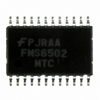
FMS6502MTC24 Fairchild Semiconductor, FMS6502MTC24 Datasheet

FMS6502MTC24
Specifications of FMS6502MTC24
Available stocks
Related parts for FMS6502MTC24
FMS6502MTC24 Summary of contents
Page 1
... Automotive (In-Cabin Entertainment) Ordering Information Part Number Pb-Free FMS6502MTC24 Yes FMS6502MTC24X Yes © 2006 Fairchild Semiconductor Corporation Rev. 1.0.0 Description The FMS6502 provides eight inputs that can be routed to any of six outputs. Each input can be routed to one or more outputs, but only one input may be routed to any output ...
Page 2
... FAIRCHILD IN2 3 FMS6502 VDD 4 24L TSSOP IN3 5 GND 6 IN4 7 ADDR1 8 IN5 9 ADDR0 10 IN6 11 SCL 12 Figure 2. Pin Configuration © 2006 Fairchild Semiconductor Corporation FMS6502 Rev. 1.0.0 Pin Description Pin# Pin GND 24 1 IN1 2 GND 23 OUT1 3 IN2 OUT2 22 4 VDD 5 IN3 OUT3 21 6 GND ...
Page 3
... Absolute Maximum Ratings. Symbol T Operating Temperature Range A V Supply Voltage Range CC Electrostatic Discharge Information Symbol HBM Human Body Model (JEDEC: JESD22-A114) CDM Charged Device Model (JEDEC: JESD22-A101) © 2006 Fairchild Semiconductor Corporation FMS6502 Rev. 1.0.0 Min. -0.3 -0.3 Parameter Parameter Parameter 3 Max. Unit ...
Page 4
... Note: 1. When the OFF input selection is used, the output amplifier is powered down and enters a high-impedance state. © 2006 Fairchild Semiconductor Corporation FMS6502 Rev. 1.0.0 0110) with the ability to offset based upon the values of the ADDR0 and ADDR1 inputs. Offset addresses are ...
Page 5
... Adjacent input pair to adjacent output pair. Interfering input is through a closed switch. 4. Crosstalk of eight synchronous switching outputs onto single, asynchronous switching output. 5. SNR = 20 * log (714mV / rms noise). © 2006 Fairchild Semiconductor Corporation FMS6502 Rev. 1.0.0 , input bias mode, one-to-one routing, 6dB gain, all inputs AC-coupled with 0.1μF, ...
Page 6
... Start Set-up Time following a Stop BUF t Start Hold Time HD,STA t Start Set-up Time following Clock Low to High SU,STA Note: 1. 100% tested at 25°C. SDA t BUF SCL SDA © 2006 Fairchild Semiconductor Corporation FMS6502 Rev. 1.0.0 . Conditions SDA,SCL,ADDR SDA,SCL,ADDR SCL 1. 1. LOW HD,STA HD,DAT ...
Page 7
... A HIGH-to-LOW transition of the data line, while the clock is HIGH, is defined as start condition (S). SCL S SDA START condition © 2006 Fairchild Semiconductor Corporation FMS6502 Rev. 1.0 specifi- Bit Transfer One data bit is transferred during each clock pulse. The data on the SDA line must remain stable during the HIGH period of the clock pulse ...
Page 8
... Fairchild Semiconductor Corporation FMS6502 Rev. 1.0.0 The device that acknowledges must pull down the SDA line during the acknowledge clock pulse so the SDA line is stable LOW during the HIGH period of the acknowl- edge-related clock pulse (set-up and hold times must be taken into consideration) ...
Page 9
... Video source must be AC coupled 75 Figure 9. Bias Mode Input Circuit © 2006 Fairchild Semiconductor Corporation FMS6502 Rev. 1.0.0 Output Configuration The FMS6502 outputs may DC-coupled. DC- coupled loads can drive a 150Ω load. AC-coupled out- puts are capable of driving a single, doubly terminated 2 C-compatible interface ...
Page 10
... IN1 to any output. For output crosstalk, the switch is closed. Crosstalk from OUT1 to any output is measured. © 2006 Fairchild Semiconductor Corporation FMS6502 Rev. 1.0.0 Crosstalk from multiple sources into a given channel is measured with the setup shown in Figure 14. Input In1 is ...
Page 11
... Maximize thermal performance of the PCB. • Consider using 70µm of copper for high-power designs. © 2006 Fairchild Semiconductor Corporation FMS6502 Rev. 1.0.0 • Make the PCB as thin as possible by reducing FR4 thickness. • Use vias in power pad to tie adjacent layers together. ...
Page 12
... Physical Dimensions Dimensions are in millimeters unless otherwise noted. Figure 15. 24-Lead Thin Shrink Small Outline Package © 2006 Fairchild Semiconductor Corporation FMS6502 Rev. 1.0.0 12 www.fairchildsemi.com ...
Page 13
... Fairchild Semiconductor Corporation FMS6502 Rev. 1.0.0 13 www.fairchildsemi.com ...


